

 Printed Circuit Boards
 Surface
 PCB Assembly
 Layer Buildup
 Online Tools
 PCB Design-Aid & Layout
 Mechanics
 SMD-Stencils
 Quality
 Drills & Throughplating
 Factory & Certificate


-

-
-
-
-
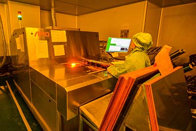
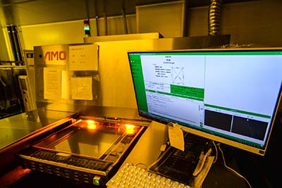
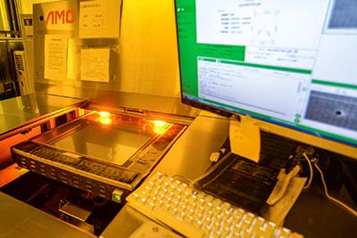
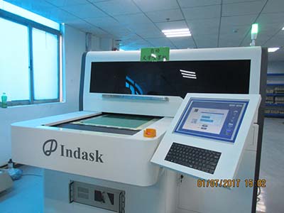
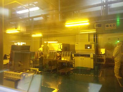
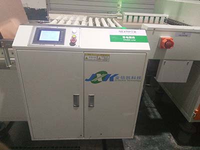
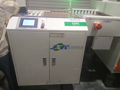
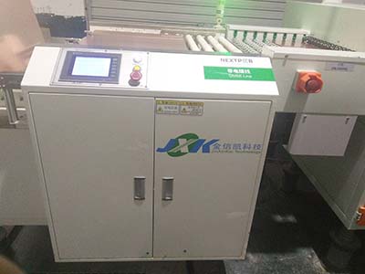
Light painting operation--photographing system
The process is as shown below: (PCB/LCD design)-->(CAM system)-->(Gerber file)
3541 1 0 Shares
-
-
-
-
-
-
-
PCB Design Principles
Eight Principles of PCB Design
3978 1 0 Shares
-
-
PCB design skills based on GENESIS2000 software (2)
Part 6-12
5273 5 0 Shares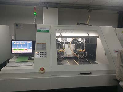
-
PCB design skills based on GENESIS2000 software (1)
Part 1-5
4207 1 0 Shares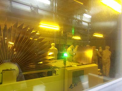
-
-
-
-
-
Categories
Recommended Article:
- Exploring the Significance of Drill Holes in PCB Manufacturing
- From Prototype to Mass Production: The Role of Golden Boards in PCB Industry
- Unveiling the Characteristics and Implementation of Flip Chip Bonding Technology
- DFRobot x NextPCB LattePanda MU Carrier Board Design Challenge - NextPCB Accelerator #9
- Unlock Open-Source FPGA Innovation with Tang Primer 25K from Sipeed - NextPCB Accelerator #8
- Top 9 Most Common IC Packaging Types in Modern Electronics
- Harnessing the SIM7600's Full Potential: A Systems-Level Perspective
- Comprehensive Comparison of PCB Additive and Subtractive Methods
- Deploy Smarter IoT solutions with SIM7600 4G LTE Modules and Free Prototypes - NextPCB Accelerator #7
- Understanding the Differences Between CPU, MCU, MPU, SoC, DSP, ECU, GPU, and FPGA
