Panel Creation
Posted: 09:45 AM December 24, 2019
writer: NextPCB
What is the PCB panel?
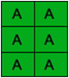
Panel creation means that multiple circuit boards are combined in a single large board to form a “panel.” For the sake of cost-saving, repeatability, and machinery, PCB manufacturers always suggest customers design panel in PCB fabrication and PCB assembly process unless the board is large or requires special processing. Panel creation helps to save time and cost through improving the efficiency and yield of fabrication, increasing material utilization.
Panel types
1. Multiplier panel: identical PCBs within a panel

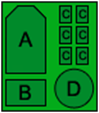
2. Mixed multiplier panel: different PCBs within a panel

How does the panel work?
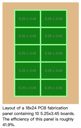
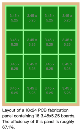
From a fixed panel cost, more boards packed into one panel means more efficiency in manufacturing and less costly. Usually, the more boards on a single panel, the lower the per-board price is. Let’s take the example (identical PCBs) below to have a clear understanding of effective panel creation.


What is the difference between this two-panel design? Rotate the boards 90 degrees can place 60% more boards on the panel with the same size. Best panel creation seems like a win-win situation for both PCB manufacturers and customers. Professional PCB fabricators will quote based on different board rotation. But maybe some manufacturers will tell you if you don' t ask.
Besides, boards with different shapes or sizes also can be easily aggregated on one board if they are manufactured in “common” technology, which is called a mixed multiplier panel. This way means the cost of manufacturing the panel can be spread among multiple customers, and the panel efficiency can be significantly improved. Cost-saving and time-saving are the essential factors in fabrication for both manufacturers and customers.
Several ways of panel design
1. V-scoring/V-cut/V-groove
V-scoring is the most popular way in PCB panel design. The space between each unit can be 0.0mm or 0.3mm for panel with V-scoring in the following picture.
2. Tab-route
The space between each board needs to be 1.6mm for panel with tab-route, and there are two types of tab-route as below:
① Tab-route with breaking holes (stamp holes)
② Tab-route with the tab (no holes)
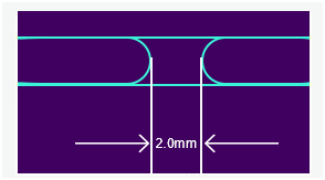
The space between each tab should be 2.0mm as the flowing picture.

3. Combination of V-scoring/V-cut/V-groove and Tab-route
The space between each board should be 2.0mm when panel with both V-cut and tab-route. This combination way usually increases the production cost but reduces PCBA separating labor and lower the damage risk.
For the best use of the available space on a panel, customers need to learn more about the details of the panel size the PCB manufacturers usually use. The minimum size of the PCB assembly panel in NextPCB is 50mm*50mm; the maximum size is 600mm*500mm. Customers can provide panel data, or NextPCB can provide the panel design according to customers' requirements. If you are still unclear about the panel creation, please feel free to leave messages or send Emails to support@nextpcb.com for further consultation.
 PCB Assembly
 Layer Buildup
 Online Tools
 PCB Design-Aid & Layout
 Mechanics
 SMD-Stencils
 Quality
 Drills & Throughplating
 Factory & Certificate
 PCB Assembly Factory Show
Certificate

