Layer Orientation
Posted: 08:10 PM December 19, 2019
writer: NextPCB
Layer orientation, also called layer labeling, is main to avoid mirrored layers. For correct and efficient production of printed circuit boards (PCBs), manufacturers must label the copper of the top and bottom layer, even each inner layer when it comes to multilayers boards. PCB manufacturers always use TOP and BOT as a uniform inscription to indicate the top layer and the bottom layer.
The importance of labeling all the layers separately
Incorrect or missing label during the production process is the most common reason for the problem. Because many layout programs permit mirrored data output. Therefore, it is crucial to label boards in the copper with TOP and BOT. Marking the TOP and BOT of copper on boards can provide information about layer orientation and layer definitions. Layer definition means the unique labeling of the top and the bottom layers.
1. The situation of no label in the copper
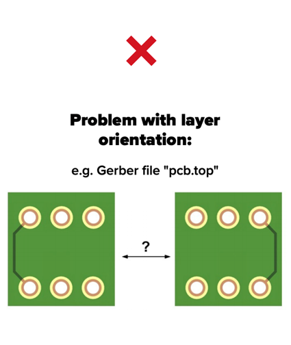
Please see the following picture, can you distinguish the right orientation of the layer?

From the above picture, we will know that even the Gerber file data defines which layer the top or the bottom layer is, the layer orientation still cannot be determined without a label inscription in the copper. Because almost every AD program allows mirrored output data, even for single-sided PCBs. This situation applies worldwide for every PCB manufacturers.
2. The situation of the correct label for layer orientation
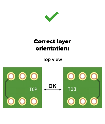
Now let' s see the right layer orientation in the following picture.

Correct layer orientation means the label should appear in the copper in the layout program, as shown in the above image. The label "TOP" should be legible, and the word "BOT" on the bottom layer should be mirrored from the top view. And "BOT" will be readable once the board is finished.
3. Layer orientation for multilayers
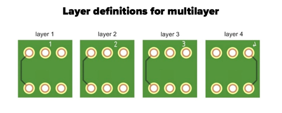
For the multilayers, continuous labeling is recommended for each layer in the following picture. And the label for the bottom layer should be mirrored when viewing from above. (The "layer 1" to "layer 4" on the top of the picture are shown only for clarity)

Each layer must be clearly labeled, and it is better to attach a readable text on each layer (inside or outside the board). The texts need to be subject to design rules for traces and must be etched as well as traces.
In a word, layer definition and layer orientation are significant for correct production in the PCB prototype and PCB assembly process. Customers need to mark each layer correctly when designing the layout of PCBs to avoid confusion during the fabrication process.
 PCB Assembly
 Layer Buildup
 Online Tools
 PCB Design-Aid & Layout
 Mechanics
 SMD-Stencils
 Quality
 Drills & Throughplating
 Factory & Certificate
 PCB Assembly Factory Show
Certificate

