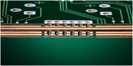
Thick-copper PCBs
Posted:10:49 AM December 11, 2019
writer: NextPCB
In normal conditions, the copper foil thickness in standard PCBs is 1oz -3oz. Thick-copper PCB, also known as heavy-copper PCBs, it is a unique type of PCB that the finished copper weight is more than 4oz, and the copper thickness above 20oz is regarded as extreme copper PCB.

The specialties of thick-copper PCBs
Most of the thick-copper PCBs are high current substrates, and the main application areas are power supply module and automotive electrics. The main terminal electronic products filed by thick-copper PCBs are diverse. Some are the same as conventional PCB, such as portable electronic products, network products, and base station equipment; some are different from the conventional PCB field, such as automotive industry control, power module.
Standard PCBs are fabricated using a combination of copper etching and plating processes. Thick-cooper PCBs use the same manufacturing way with special etching and electroplating technology. And they differ in efficacy. The primary function of conventional PCBs is to construct the wires(wiring) that carry signals. The primary purpose of the thick-copper substrate carrying power devices with large current passing through is to protect the current-carrying capacity and to stabilize the power supply.
The development trend of high-current substrates is that the heat emitted by devices with larger currents need to dissipate. Therefore, the large current passed is getting larger, and the thickness of the copper foil used for the substrate is getting thicker. The thick-cooper PCBs allow the rapid development of power electrics products.
Benefits of thick-copper PCBs
- High current carrying capacity
- Great endurance to thermal strains
- Reduce the size(volume) of end products through incorporating multiple copper weights on the same layer of the circuit board
- Increase the mechanical strength at connector sites and in PTH holes
- Excellent heat dissipation efficiency
The significant of application function of thick-copper PCBs
In recent years, as the result of high power requirements, the demands for thick-cooper PCBs have been increased considerably. Due to the excellent performance in high current applications, heat dissipation of components with massive power loss, thermal distribution for excellent thermal management. Heavy copper PCBs always used for computers, high power rectifiers, military, power grid switching systems, electric vehicle charging, etc. The new expansion of thick-copper application functions has driven the development of the market, mainly in the following aspects:
1. The advantages of miniaturizations, thinning, and multi-layers of thick-copper PCBs are full display, which accelerates the pace of replacing ceramic substrates.
2. The advancement of design and manufacturing technology of thick-copper PCBs has promoted the "integration" of the power circuit and control circuit.
3. The diversified thick-copper PCB structures improve the heat dissipation of overall products, which offer more possibilities for the research and development of high-density and high-power products.
As a professional PCB manufacturer, NextPCB has more than ten years of experience in fabricating and assembling thick-copper and high-performance PCB products. The strict quality control system and the high-tech operating procedure can help customers achieve productivity and high-quality goals, and ensure the end electronic boards meet the quality and performance expectations.
 PCB Assembly
 Layer Buildup
 Online Tools
 PCB Design-Aid & Layout
 Mechanics
 SMD-Stencils
 Quality
 Drills & Throughplating
 Factory & Certificate
 PCB Assembly Factory Show
Certificate


