

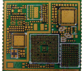
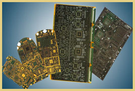
 Printed Circuit Boards
 Surface
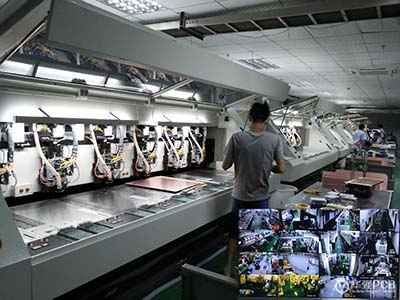
 PCB Assembly
 Layer Buildup
 Online Tools
 PCB Design-Aid & Layout
 Mechanics
 SMD-Stencils
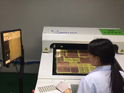
 Quality
 Drills & Throughplating
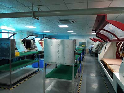
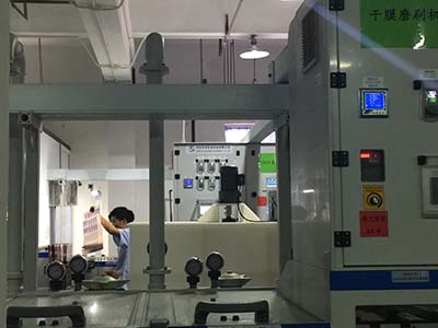
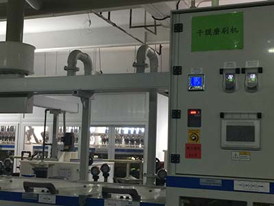
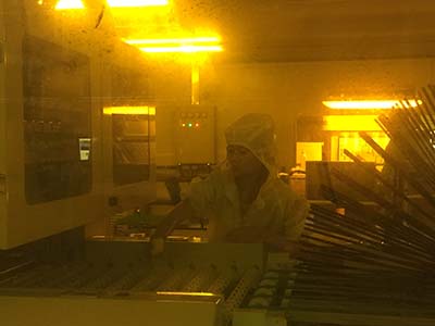
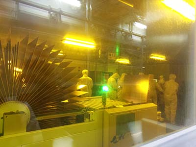
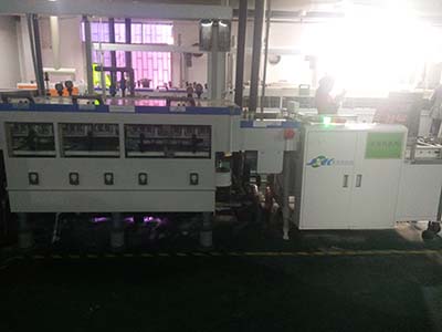
 Factory & Certificate


-

-
-
-
-
-
-
PCB design tips 100, teach you to master PCB design easily (66-75)
PCB design tips-teach you to master PCB design easily (66-75)
2892 1 0 Shares
-
PCB design tips 100, teach you to master PCB design easily (56-65)
PCB design tips 100, teach you to master PCB design easily
2866 2 0 Shares
-
PCB design tips 100, teach you to master PCB design easily (46-55)
PCB design tips-teach you to master PCB design easily
2885 1 0 Shares
-
-
-
PCB design tips 100, teach you to master PCB design easily (19-24)
In this article we will teach you how to do a PCB design easily(19-24)
2833 3 0 Shares
-
PCB design tips 100, teach you to master PCB design easily (11-18)
In the high-speed PCB design, teach your PCB design easily. (11-18)
2603 5 0 Shares
-
-
-
-
India Customer pls provide POA /KYC required
India Customer pls provide POA /KYC required for order PCB in NEXTPCB Manufacturer.
6298 0 0 Shares
-
Freight Discount Promotion Notice
3160 0 0 Shares
-
-

Categories
Recommended Article:
- From Prototype to Mass Production: The Role of Golden Boards in PCB Industry
- Unveiling the Characteristics and Implementation of Flip Chip Bonding Technology
- DFRobot x NextPCB LattePanda MU Carrier Board Design Challenge - NextPCB Accelerator #9
- Unlock Open-Source FPGA Innovation with Tang Primer 25K from Sipeed - NextPCB Accelerator #8
- Top 9 Most Common IC Packaging Types in Modern Electronics
- Harnessing the SIM7600's Full Potential: A Systems-Level Perspective
- Comprehensive Comparison of PCB Additive and Subtractive Methods
- Deploy Smarter IoT solutions with SIM7600 4G LTE Modules and Free Prototypes - NextPCB Accelerator #7
- Understanding the Differences Between CPU, MCU, MPU, SoC, DSP, ECU, GPU, and FPGA
- RAK3172: The Ultimate LoRaWAN Module for IoT Applications in 2025
