

 Printed Circuit Boards
 Surface
 PCB Assembly
 Layer Buildup
 Online Tools
 PCB Design-Aid & Layout
 Mechanics
 SMD-Stencils
 Quality
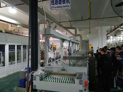
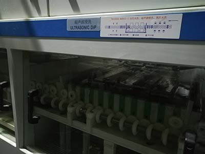
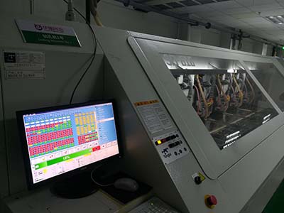
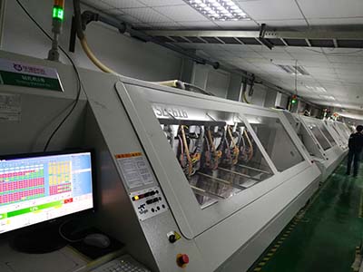
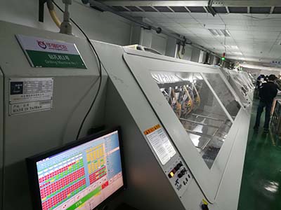
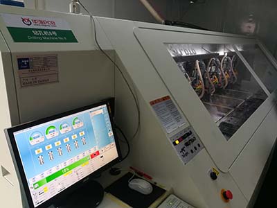
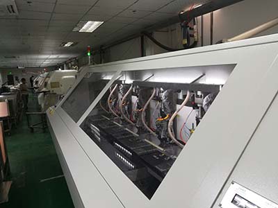
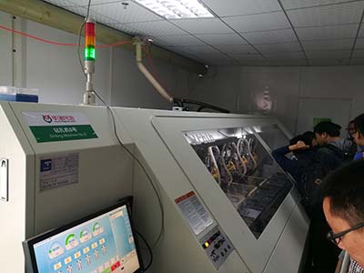
 Drills & Throughplating
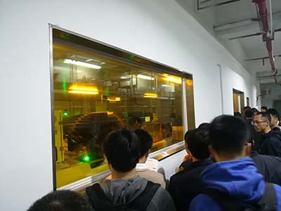
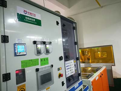
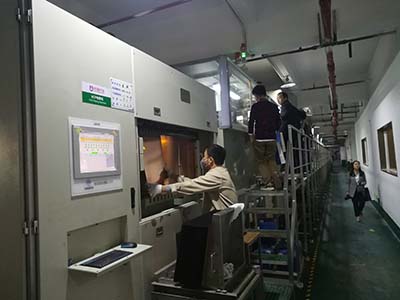
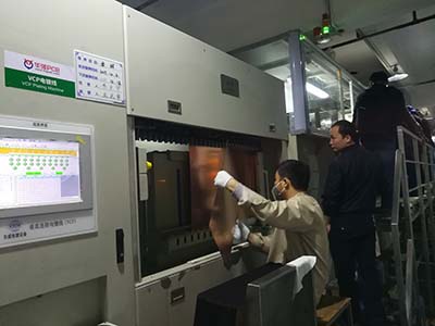
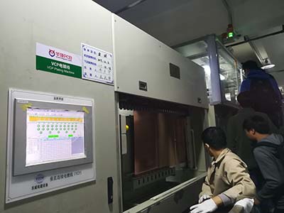
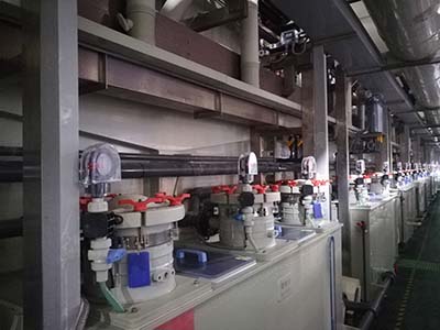
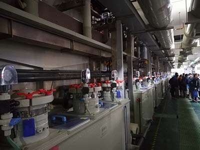
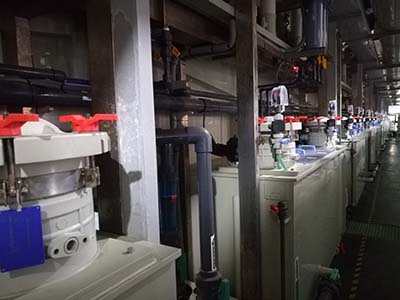
 Factory & Certificate


-
-
-
-
Capacitor detection method and experience
The following is an introduction to the testing experience and methods of capacitors.
3661 5 0 Shares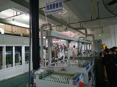
-
Resistor detection method and experience
The following is an introduction to the testing experience and methods of resistors.
3551 2 0 Shares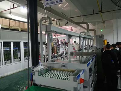
-
-
-
-
-
-
-
-
-
Correct differential pair routing method in Altium 9
How to define differential pairs in the schematic
5686 6 0 Shares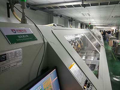
-
-
-
-
-
-
Categories
Recommended Article:
- From Prototype to Mass Production: The Role of Golden Boards in PCB Industry
- Unveiling the Characteristics and Implementation of Flip Chip Bonding Technology
- DFRobot x NextPCB LattePanda MU Carrier Board Design Challenge - NextPCB Accelerator #9
- Unlock Open-Source FPGA Innovation with Tang Primer 25K from Sipeed - NextPCB Accelerator #8
- Top 9 Most Common IC Packaging Types in Modern Electronics
- Harnessing the SIM7600's Full Potential: A Systems-Level Perspective
- Comprehensive Comparison of PCB Additive and Subtractive Methods
- Deploy Smarter IoT solutions with SIM7600 4G LTE Modules and Free Prototypes - NextPCB Accelerator #7
- Understanding the Differences Between CPU, MCU, MPU, SoC, DSP, ECU, GPU, and FPGA
- RAK3172: The Ultimate LoRaWAN Module for IoT Applications in 2025
