

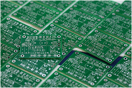
 Printed Circuit Boards
 Surface
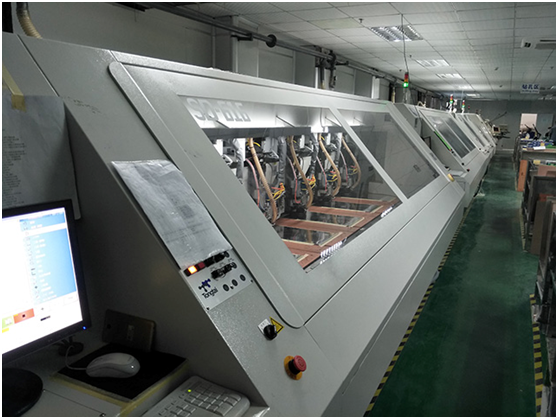
 PCB Assembly
 Layer Buildup
 Online Tools
 PCB Design-Aid & Layout
 Mechanics
 SMD-Stencils
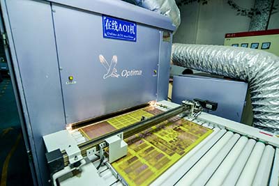
 Quality
 Drills & Throughplating
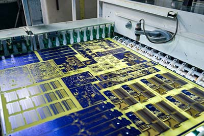
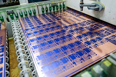
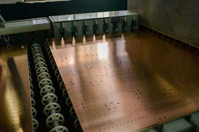
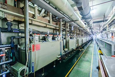
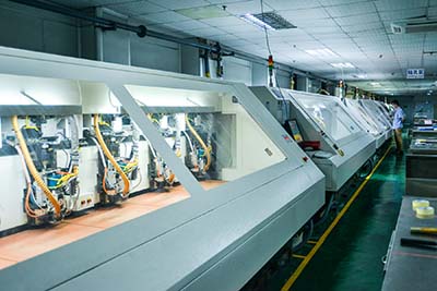
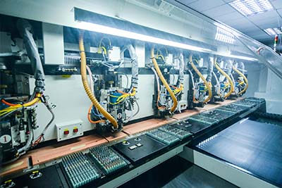
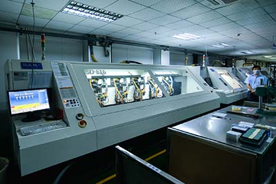
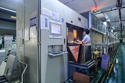
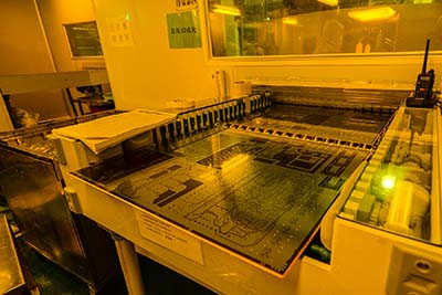
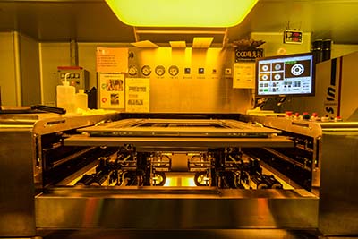
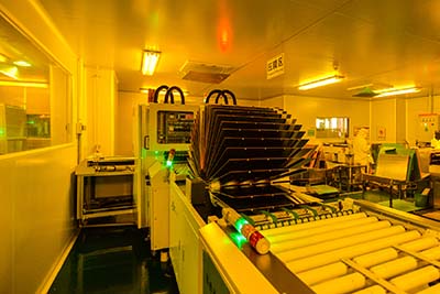
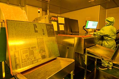
 Factory & Certificate


-
-
-
-
-
-
-
-
-

-
-
-
-

-
Payment Matters
3874 0 0 Shares
-
-
-
-
-
-

Categories
Recommended Article:
- NextPCB Unveils New Logo Reflecting Commitment to Innovation and Enhanced Customer Service
- Exploring the Significance of Drill Holes in PCB Manufacturing
- From Prototype to Mass Production: The Role of Golden Boards in PCB Industry
- Unveiling the Characteristics and Implementation of Flip Chip Bonding Technology
- DFRobot x NextPCB LattePanda MU Carrier Board Design Challenge - NextPCB Accelerator #9
- Unlock Open-Source FPGA Innovation with Tang Primer 25K from Sipeed - NextPCB Accelerator #8
- Top 9 Most Common IC Packaging Types in Modern Electronics
- Harnessing the SIM7600's Full Potential: A Systems-Level Perspective
- Comprehensive Comparison of PCB Additive and Subtractive Methods
- Deploy Smarter IoT solutions with SIM7600 4G LTE Modules and Free Prototypes - NextPCB Accelerator #7
