

 Printed Circuit Boards
 Surface
 PCB Assembly
 Layer Buildup
 Online Tools
 PCB Design-Aid & Layout
 Mechanics
 SMD-Stencils
 Quality
 Drills & Throughplating
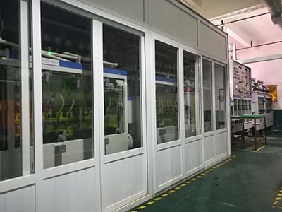
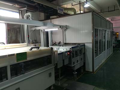
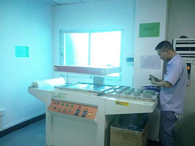
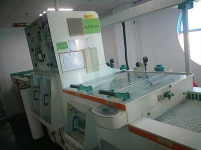
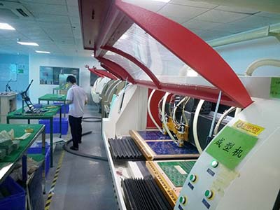
 Factory & Certificate


-
The golden rule that PCB design never changes
10 Rules
3402 1 0 Shares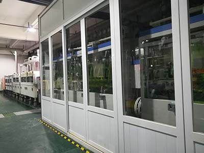
-
PCB design technology
PCB design techniques have an impact on the following three effects:
3697 1 0 Shares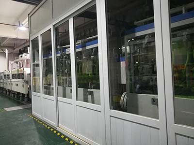
-
-
-
-
PCB layout design view elements
55 elements
3515 1 0 Shares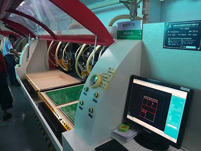
-
-
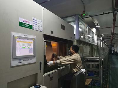
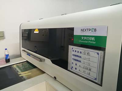
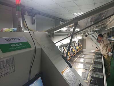
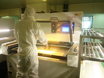
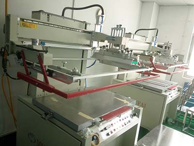
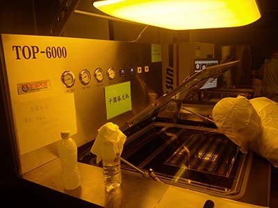
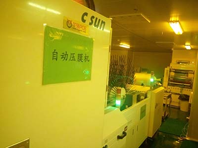
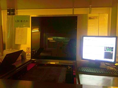
PCB basic manufacturing process
The PCB manufacturing process begins with a "substrate" made of Glass Epoxy or similar material.
3383 1 0 Shares
-
-

-
-
-
-
-
-
-
-
-
-
Categories
Recommended Article:
- DFRobot x NextPCB LattePanda MU Carrier Board Design Challenge - NextPCB Accelerator #9
- Unlock Open-Source FPGA Innovation with Tang Primer 25K from Sipeed - NextPCB Accelerator #8
- Top 9 Most Common IC Packaging Types in Modern Electronics
- Harnessing the SIM7600's Full Potential: A Systems-Level Perspective
- Comprehensive Comparison of PCB Additive and Subtractive Methods
- Deploy Smarter IoT solutions with SIM7600 4G LTE Modules and Free Prototypes - NextPCB Accelerator #7
- Understanding the Differences Between CPU, MCU, MPU, SoC, DSP, ECU, GPU, and FPGA
- RAK3172: The Ultimate LoRaWAN Module for IoT Applications in 2025
- Build Low-Cost FPGA Projects with Tang Nano 20K and Free PCBA Prototypes - NextPCB Accelerator #6
- NextPCB DFM Tool Exclusive Offer: Get a $10 Coupon Every Month!
