PCB milling
Posted: 09:42 AM December 27, 2019
writer: NextPCB
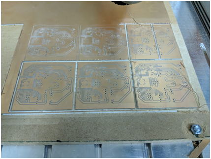
PCB milling is the process of using a tooler to mill the inner and the outer contour of the board. In normal conditions, the PCB breakaway and outline are milled and do not need extra charge if there is no special requirement for the milling.

The importance of the mechanical layer data for an excellent PCB milling
For a perfect PCB production, the correct mechanical layer data file in the Gerber file is very important. All the required mechanical information for all layers should be included in the data file to produce the boards.
l The mechanical layer data should contain the following information:
1. Precise circuit board outline, preferably including dimensions (inch or mm)
2. Precise positioning and the position and the size of all internal milling, slots, or cutouts, preferably including dimensions (inch or mm)
Please pay attention to that, do not scale the mechanical layer, keep it 1 to 1 and indicate the accurate dimensions of the PCB.
l Milling data in the mechanical layer
The routing and milling data is production-specific and depends on the hob tools, toll offsets, routing order, and orientation used by each PCB manufacturer. Therefore, there is no need to provide the actual routing and milling layers of the board outline and internal cutouts. PCB manufacturers need to recreate routing and milling layers completely, although the confusion or misunderstanding will exist and lead to incorrect boards. As a professional PCB manufacturer, it is the essential capability to prepare the correct production process routing and milling layer by using the information in the mechanical layer.
Some design tips in PCB milling
1. The standard tool size for all contour routing or milling is 2.0mm, which means the standard minimum radius of the inside corners is 1.0mm.
2. The requirement for a smaller internal radius should be clearly indicated in the mechanical layer.
3. If you need sharpness or a 90-degree internal angle, you can get this drill by placing an adequately sized NPTH bit in the center of the board contour at the internal angle or by cleverly designing the circuit board contour.
4. The inner and outer contours of the board should be marked with a line width of 1 μm to prevent the measurement and size issues.
5. If the dimensions of the outlines and milling sizes are not given in the mechanical layer, we can use the center of the contour line as the precise contour of the board regardless of its thickness.
6. It is vital to avoid copper when milling the board for the durability of the PCB.
The mechanical layer is essential for the milling in the PCB production process. And except for milling data, there are some additional information should be included in the mechanical layer data, such as drill position symbols, reference hole, PTH/NPTH indication, customer panels, layer sequence, and special buildups, etc. No matter the PCB prototype or the PCB mass production, the production process is a complex and delicate process. Customers need to concern the capability of a PCB manufacturer as well as the cost of PCB fabrication. NextPCB is the best choice if you have a PCB project
 PCB Assembly
 Layer Buildup
 Online Tools
 PCB Design-Aid & Layout
 Mechanics
 SMD-Stencils
 Quality
 Drills & Throughplating
 Factory & Certificate
 PCB Assembly Factory Show
Certificate


