

 Printed Circuit Boards
 Surface
 PCB Assembly
 Layer Buildup
 Online Tools
 PCB Design-Aid & Layout
 Mechanics
 SMD-Stencils
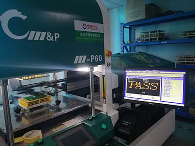
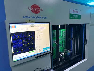
 Quality
 Drills & Throughplating
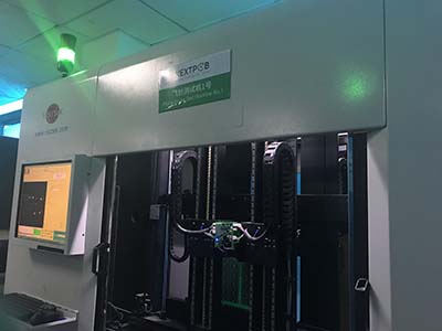
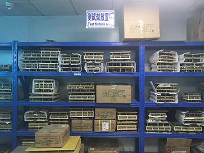
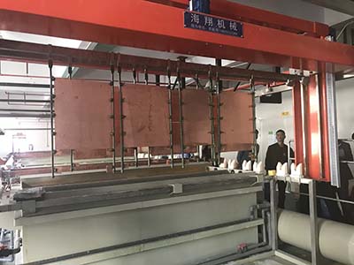
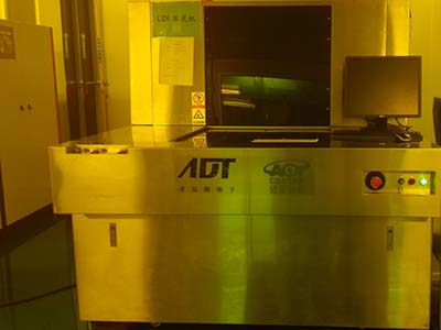
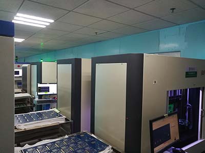
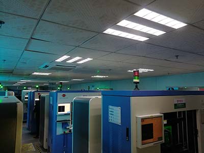
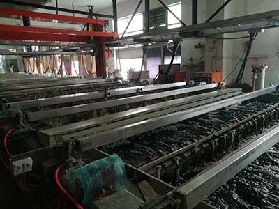
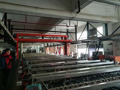
 Factory & Certificate


-
-
-

-
-
Nine standards for RF in PCB design
Nine standards for RF in PCB design,mainly use 4-6 layers.
3766 3 0 Shares
-
-
-
Special Offers Cannot Use Coupons and Points
3272 0 0 Shares
-
-
-
-
-
PCB process skills based on GENESIS2000 software (3)
7. Solder mask 8. BGA plug hole 9. Network comparison 10. Character layer
4206 2 0 Shares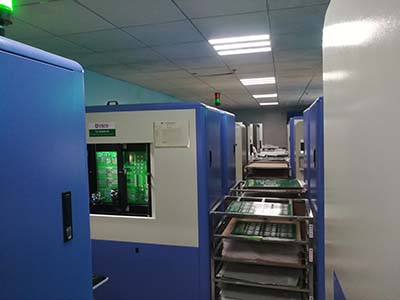
-
PCB process skills based on GENESIS2000 software (2)
4. Drilling Editing 5. Drilling Outline Drawing 6. Circuit Layer
3673 1 0 Shares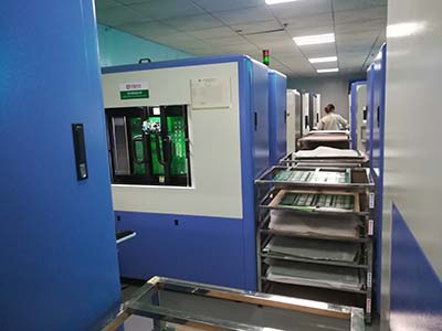
-
-
-
-
-

-

Categories
Recommended Article:
- Unveiling the Characteristics and Implementation of Flip Chip Bonding Technology
- DFRobot x NextPCB LattePanda MU Carrier Board Design Challenge - NextPCB Accelerator #9
- Unlock Open-Source FPGA Innovation with Tang Primer 25K from Sipeed - NextPCB Accelerator #8
- Top 9 Most Common IC Packaging Types in Modern Electronics
- Harnessing the SIM7600's Full Potential: A Systems-Level Perspective
- Comprehensive Comparison of PCB Additive and Subtractive Methods
- Deploy Smarter IoT solutions with SIM7600 4G LTE Modules and Free Prototypes - NextPCB Accelerator #7
- Understanding the Differences Between CPU, MCU, MPU, SoC, DSP, ECU, GPU, and FPGA
- RAK3172: The Ultimate LoRaWAN Module for IoT Applications in 2025
- Build Low-Cost FPGA Projects with Tang Nano 20K and Free PCBA Prototypes - NextPCB Accelerator #6
