
 PCB Assembly
 Layer Buildup
 Online Tools
 PCB Design-Aid & Layout
 Mechanics
 SMD-Stencils
 Quality
 Drills & Throughplating
 Factory & Certificate
 PCB Assembly Factory Show
Certificate
PCB Assembly Factory Show
Certificate
Support Team
Feedback:
support@nextpcb.comThis article delves into the features, implementation process, and detailed techniques of Flip Chip Bonding (FCB) technology, a cornerstone in advanced PCB assembly and semiconductor packaging.
Flip Chip Bonding (FCB) and Flip Chip technology essentially refer to the process where a semiconductor die is mounted face-down, directly interconnected to the substrate's contact pads via an array of solder bumps. In contrast, when a chip is interconnected to a substrate using wire bonding, the chip faces upwards – a configuration commonly known as face-up mounting. This stands in stark contrast to wire bonding (WB) and tape automated bonding (TAB). FCB eliminates the need for traditional interconnecting wires, significantly reducing interconnect capacitance and inductance, making it particularly well-suited for high-frequency and high-speed electronic products.
Furthermore, by occupying a smaller substrate area, it substantially increases chip mounting density, establishing it as a preferred solution for Large-Scale Integration Circuits (LSICs), Very-Large-Scale Integration Circuits (VLSICs), and Application-Specific Integrated Circuits (ASICs). A key advantage of FCB technology is that chip mounting and interconnection are completed simultaneously, greatly simplifying the manufacturing process and aligning with the high-volume production demands of modern Surface Mount Technology (SMT) lines.
Compared to face-up mounted chips (using wire bonding), flip chips, with their "face-down" orientation, offer significant advantages in terms of size, reliability, cost, and flexibility. The concurrent chip mounting and interconnection in FCB assembly streamline the process, making it faster and more time-efficient, ideal for industrialized, large-scale PCB manufacturing using advanced SMT equipment.
However, FCB technology also presents certain challenges. The face-down mounting and interconnection of the chip introduce complexity to the process, and solder joints cannot be visually inspected directly (requiring infrared and X-ray inspection). Additionally, the formation of bumps on the chip's bonding pads adds steps and cost to the chip manufacturing process. The thermal stress issues arising from the coefficient of thermal expansion (CTE) mismatch between interconnect materials also remain a challenge.
Nevertheless, with its increasing adoption and continuous advancements in process technology and reliability research, the challenges associated with FCB are being progressively addressed. As a wafer-level area array packaging technology, flip chip utilizes a face array bump structure for the chip's I/O interfaces, achieving exceptionally high packaging density. This area array packaging technique represents a significant revolution in packaging technology since SMT, powerfully driving the widespread adoption of high-performance mobile terminals and personal electronic devices.
Despite its advancements, FCB assembly still faces several limitations:
1. High Process Complexity and Inspection Difficulty: The face-down mounting of the chip demands stringent operational precision, requiring high-accuracy equipment for micron-level alignment. Solder joints are obscured by the chip, preventing direct visual inspection and necessitating reliance on non-contact methods like infrared or X-ray, which are costly and have limited efficiency. This impacts the overall PCB manufacturing quality assurance process.
2. Increased Manufacturing Costs: The pre-fabrication of bumps (such as gold or copper bumps) on the chip's bonding pads introduces additional photolithography and electroplating steps, significantly extending the chip manufacturing cycle and increasing production costs, ultimately affecting the cost-effectiveness of PCB prototypes utilizing this technology.
3. Significant Thermal Stress Issues: The mismatch in the Coefficient of Thermal Expansion (CTE) between the chip, bump materials, and the substrate induces substantial thermal stress, particularly in high-temperature operating conditions (200°C+) common in wide-bandgap semiconductor devices. This can lead to solder joint fatigue cracking and reduced long-term reliability, and a complete solution is yet to be established, impacting the long-term performance of PCB assemblies using flip chip.
However, with the increasing penetration of FCB technology in consumer electronics and communication sectors, ongoing research focused on process optimization and reliability enhancement continues to advance. The emergence of novel inspection techniques, material innovations, and improved process solutions in recent years is gradually overcoming these technical bottlenecks, propelling FCB towards greater maturity in advanced PCB manufacturing.
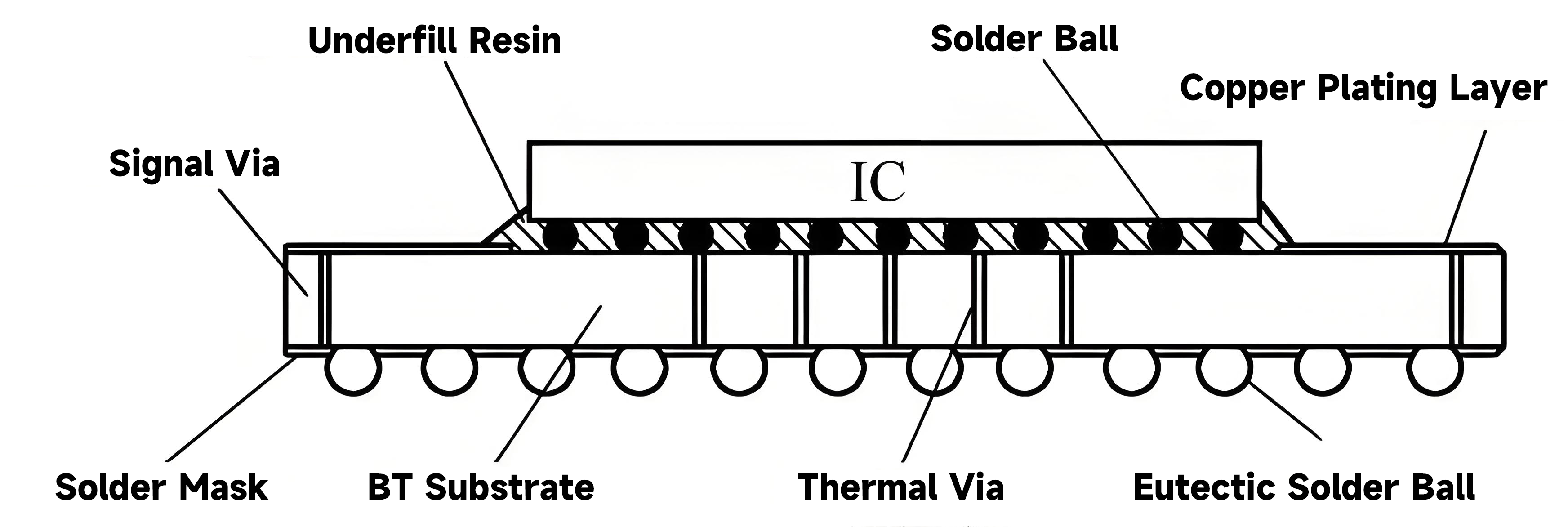
Flip Chip Package Structure Diagram
To date, flip chip technology has addressed some of its earlier challenges:
Despite the progress, several challenges still need to be addressed in flip chip technology and its application in PCB manufacturing:
By addressing these remaining challenges through continued research and development in materials, processes, and inspection techniques, flip chip technology will continue to evolve as a critical enabler for high-performance and miniaturized electronic devices across various industries, driving innovation in PCB design, PCB manufacturing, and PCB assembly.
Still, need help? Contact Us: support@nextpcb.com
Need a PCB or PCBA quote? Quote now
|
Dimensions: (mm) |
|
|
Quantity: (pcs) |
|
|
Layers: 2 |
Thickness: 1.6 mm |
|
|
|

 Printed Circuit Boards
 Surface

