
 PCB Assembly
 Layer Buildup
 Online Tools
 PCB Design-Aid & Layout
 Mechanics
 SMD-Stencils
 Quality
 Drills & Throughplating
 Factory & Certificate
 PCB Assembly Factory Show
Certificate
PCB Assembly Factory Show
Certificate
Support Team
Feedback:
support@nextpcb.comIn the field of PCB (Printed Circuit Board) manufacturing, additive and subtractive processes are two core technical approaches. They exhibit significant differences in material selection, process flow, and final product performance. This article provides a systematic comparison of the two methods from the perspectives of technical principles, process flows, advantages and disadvantages, costs, and application scenarios, helping practitioners quickly grasp the key differences and make informed decisions.
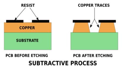
- Core Logic: Uses copper-clad laminate as the base material, removing unwanted copper layers through chemical etching (e.g., acidic or alkaline solutions) to retain the designed circuitry.
- Key Steps:
- Cutting and surface treatment of copper-clad laminate
- Pattern transfer (lamination, exposure, development)
- Removal of excess copper using acidic/alkaline etchants
- Solder mask and silkscreen printing
- Characteristics: Relies on copper layer subtraction to form conductive paths, requiring precise control of etching parameters to avoid over-etching or residual copper.
The process of multilayer pcb production
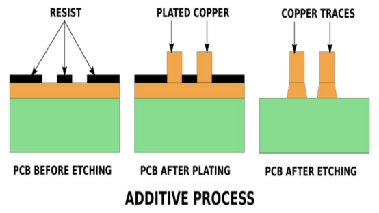
- Core Logic: Directly deposits conductive materials (e.g., copper, silver paste) onto an insulating substrate to build circuits layer by layer.
- Key Steps:
- Pretreatment of bare substrate (e.g., polyimide, ceramic)
- Selective application of photoresist or electroplating to deposit conductive layers
- Drying, curing, and removal of excess materials
- Characteristics: Eliminates the need for etching, enabling direct formation of fine traces, suitable for micro-spacing and high-density designs.
| Step | Subtractive Process | Additive Process |
| Material Preparation | Copper-clad laminate (copper foil + resin substrate) | Bare substrate (e.g., polyimide film) |
| Pattern Transfer | Photoresist coating → exposure → development → etching | Photoresist coating → exposure → development → electroplating |
| Trace Formation | Reduction of copper thickness | Addition of conductive materials |
| Post-Processing | Solder mask printing, surface treatment (OSP/HASL) | Solder mask printing, surface treatment (OSP/HASL) |
Typical Application Cases:
- Subtractive Process: Consumer electronics motherboards, appliance control boards
- Additive Process: Flexible medical sensors, high-frequency microwave substrates
- Advantages:
- High Maturity: Accounts for over 80% of market share, with a well-established supply chain.
- Cost-Effective for High Volume: Suitable for large-scale production of single/double-sided boards.
- Excellent Thermal Performance: Thicker copper layers support high-current applications.
- Limitations:
- Environmental Pressure: High costs for treating etching wastewater.
- Line Width/Spacing Limit: Approximately 20μm, unsuitable for ultra-high-density requirements.
- Poor Flexibility: Not ideal for foldable devices.
- Advantages:
- Ultra-Fine Processing: Line widths below 5μm, supporting IC substrate-level precision.
- Green Manufacturing: No copper etching waste, compliant with RoHS/REACH standards.
- Adaptability to Complex Structures: Enables 3D curved and through-hole circuits.
- Limitations:
- High Equipment Costs: Expensive plating tanks, vacuum deposition machines, etc.
- Material Constraints: Limited to non-metallic substrates (e.g., ceramics, polymers).
- Low Mass-Production Efficiency: Suitable for small batches and prototyping.
- Fixed Costs: Etching machines, exposure equipment depreciation (30% of total cost).
- Variable Costs:
- Copper Foil Waste: Higher scrap rates with finer line widths (5% increase per 0.1mm reduction).
- Etchant Consumption: Ferric nitrate solution costs ~$5/kg, with 10L hourly usage.
- Wastewater Treatment: ~$0.8 per square meter of PCB.
Case Study:
Producing 1㎡ of 4-layer FR4 board (100μm line width):
- Material cost: $12
- Processing cost: $8 (including etching, drilling)
- Total cost: $20
- Fixed Costs: Electroplating equipment, cleanroom maintenance (45% of total cost).
- Variable Costs:
- Conductive Materials: Nano-silver paste at $50/g, 0.1g per layer.
- Energy Consumption: Plating tank power at 5kW, operating cost of $0.15/h.
- Yield Loss: ~75% for complex structures (vs. 92% for subtractive process).
Case Study:
Producing 1㎡ of 6-layer ceramic substrate (20μm line width):
- Material cost: $35
- Processing cost: $18 (including sputtering, plating)
- Total cost: $53
Cost Break-Even Analysis:
For batches >500㎡, subtractive process costs 35% less. For small batches (<100㎡), additive process premiums reach 200%.
| Scenario | Recommended Process | Key Rationale |
| Consumer Electronics Motherboards | Subtractive | High volume, low cost, mature technology |
| 5G Base Station High-Frequency PCBs | Additive | Low dielectric loss, supports mmWave frequencies |
| Wearable Device Flexible Circuits | Additive | Bend cycles >100K, thickness <0.1mm |
| Automotive Control Modules | Subtractive | High-temperature resistance (150°C), vibration-proof |
| Semiconductor Package Substrates | Additive | Line width/spacing ≤50μm, supports TSV 3D packaging |
| Military/Aerospace High-Reliability PCBs | Subtractive | MIL-STD-883 certified |
- Laser Direct Structuring (LDS): Laser-activated selective copper plating.
- Green Etchants: Nitrate-free sodium persulfate systems to reduce pollution.
- Roll-to-Roll (R2R) Production: Enables continuous manufacturing of flexible substrates.
- 3D-Printed Conductive Inks: Nano-silver/copper particle direct writing, precision up to 10μm.
- Subtractive-Additive Combo: Subtractive for main traces, additive for micro-vias.
- Metal-Organic Chemical Vapor Deposition (MOCVD): Grows copper nanowire networks on substrates.
Conclusion
Choosing a PCB process is fundamentally a three-dimensional balance of cost, precision, and volume. As semiconductor packaging advances toward 2.5D/3D, additive processes will see growing adoption in high-end applications, while subtractive methods will remain dominant in traditional markets due to their mature ecosystem. Companies must establish a process evaluation matrix and dynamically adjust strategies based on product lifecycle (PLM) data. For engineers, mastering the collaborative design capabilities of both processes will be a core competency in addressing the challenges of next-generation electronics.
Still, need help? Contact Us: support@nextpcb.com
Need a PCB or PCBA quote? Quote now
|
Dimensions: (mm) |
|
|
Quantity: (pcs) |
|
|
Layers: 2 |
Thickness: 1.6 mm |
|
|
|

 Printed Circuit Boards
 Surface

