

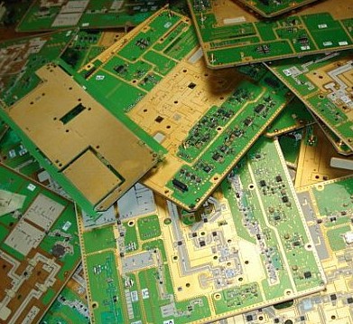
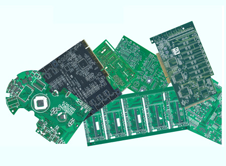
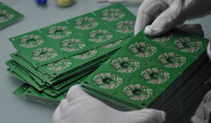
 Printed Circuit Boards
 Surface
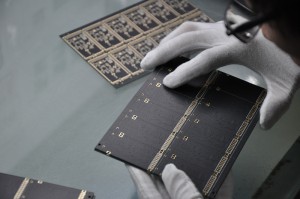
 PCB Assembly
 Layer Buildup
 Online Tools
 PCB Design-Aid & Layout
 Mechanics
 SMD-Stencils
 Quality
 Drills & Throughplating
 Factory & Certificate


-
High-speed PCB design basic concepts
To do high-speed PCB design, you must first understand the following basic concepts. This is the basis.
3659 1 0 Shares
-
CAM350 Basic Steps to Create CAM Data Summary
There are 9 steps to create Cam data by CAM350.
7918 8 0 Shares
-
-
-
-
Several misunderstandings in pcb layout learning
Seven misunderstandings in pcb layout learning
3624 1 0 Shares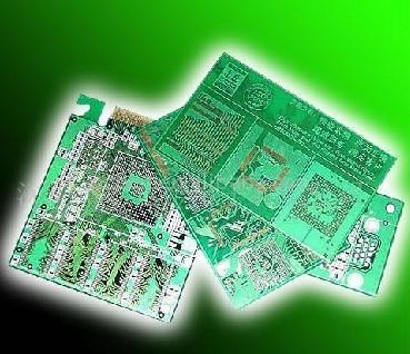
-
-
Allegro Question Set
25 Allegro questions is as fllowing.
5693 6 0 Shares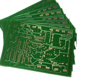
-
-
-
-

-
Price Adjustment Notice
PCB price adjustment
3581 1 0 Shares
-
-
-
-
-

-
-

Categories
Recommended Article:
- Unveiling the Characteristics and Implementation of Flip Chip Bonding Technology
- DFRobot x NextPCB LattePanda MU Carrier Board Design Challenge - NextPCB Accelerator #9
- Unlock Open-Source FPGA Innovation with Tang Primer 25K from Sipeed - NextPCB Accelerator #8
- Top 9 Most Common IC Packaging Types in Modern Electronics
- Harnessing the SIM7600's Full Potential: A Systems-Level Perspective
- Comprehensive Comparison of PCB Additive and Subtractive Methods
- Deploy Smarter IoT solutions with SIM7600 4G LTE Modules and Free Prototypes - NextPCB Accelerator #7
- Understanding the Differences Between CPU, MCU, MPU, SoC, DSP, ECU, GPU, and FPGA
- RAK3172: The Ultimate LoRaWAN Module for IoT Applications in 2025
- Build Low-Cost FPGA Projects with Tang Nano 20K and Free PCBA Prototypes - NextPCB Accelerator #6
