

 Printed Circuit Boards
 Surface
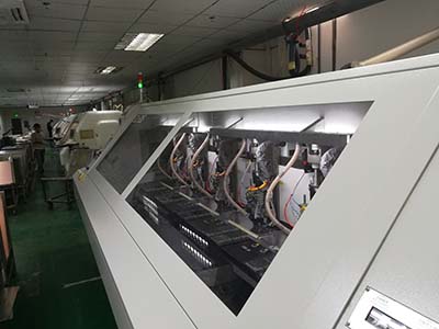
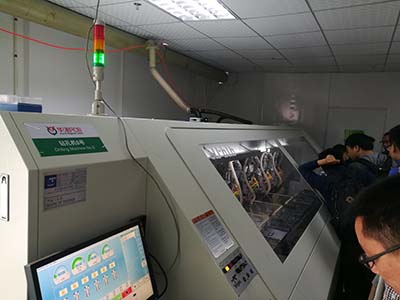
 PCB Assembly
 Layer Buildup
 Online Tools
 PCB Design-Aid & Layout
 Mechanics
 SMD-Stencils
 Quality
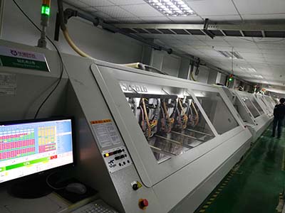
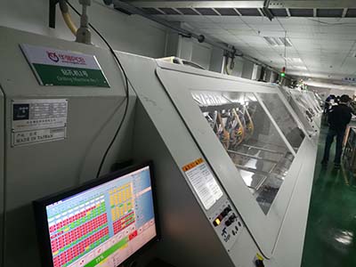
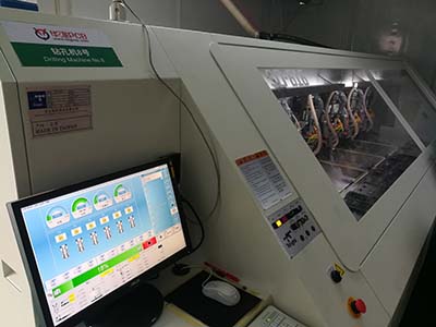
 Drills & Throughplating
 Factory & Certificate


-
Correct differential pair routing method in Altium 9
How to define differential pairs in the schematic
6049 6 0 Shares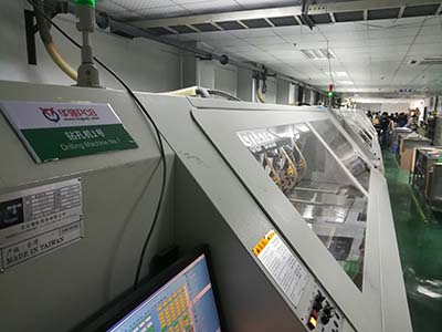
-
-
-
-
-
-
-
-
The golden rule that PCB design never changes
10 Rules
3611 1 0 Shares
-
PCB design technology
PCB design techniques have an impact on the following three effects:
3902 1 0 Shares
-
-
-
-
PCB layout design view elements
55 elements
3762 1 0 Shares
-
-
PCB basic manufacturing process
The PCB manufacturing process begins with a "substrate" made of Glass Epoxy or similar material.
3567 1 0 Shares
-
-

-
-
Categories
Recommended Article:
- Revolutionize Environmental Sensing with HP203N – Get Free PCBA Prototypes via NextPCB Accelerator #13
- How to Generate Gerbers from KiCad (Updated for KiCad 9)
- Single Layer PCBs: A Comprehensive Guide to Design, Manufacturing, and Applications
- How to convert Altium Designer files to KiCad and vice versa
- How to design your own custom PCB Ruler in KiCad
- Build Long-Range IoT Networks with Free RFM69HCW Prototypes-NextPCB Accelerator #12
- How to import Altium Libraries into KiCad (without external tools!)
- New HQDFM V4.6 Release Now Supports KiCad
- RP2040 + Cyclone 10 FPGA PCB Design Project
- KiCad 9: Design & assemble an ESP32 IoT 4-layer PCB
