

 Printed Circuit Boards
 Surface
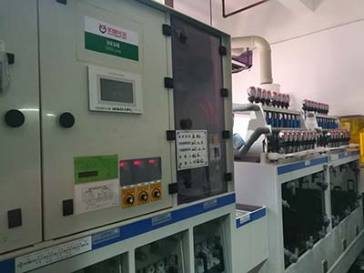
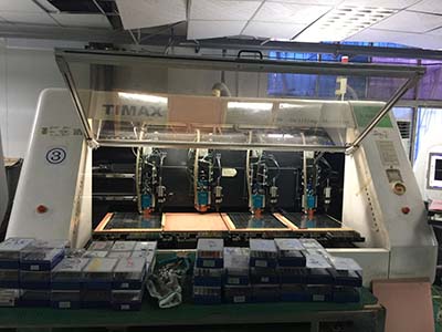
 PCB Assembly
 Layer Buildup
 Online Tools
 PCB Design-Aid & Layout
 Mechanics
 SMD-Stencils
 Quality
 Drills & Throughplating
 Factory & Certificate


-

-
-
-
-
-
-
-
-
-
-

-
-
The sale price for 4-layer PCB!!!!
Good news: A Big Sale on NextPCB, Only $28, you could own 10pcs of 4-layer PCB.
4068 4 0 Shares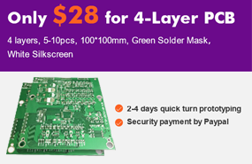
-
-
-
-
How to use Protel-39 questions and answers
There are 39 questions about how to use Protel-39 and the answers.
4472 4 0 Shares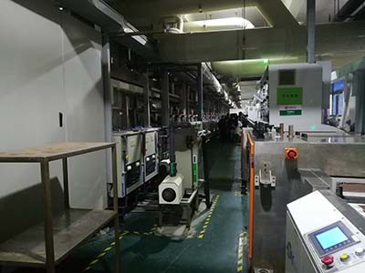
-
-
-
9 common issues with grounding
9 basic knowledge discussions about grounding technology
5737 8 0 Shares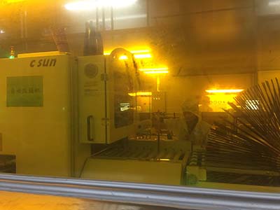

Categories
Recommended Article:
- Unveiling the Characteristics and Implementation of Flip Chip Bonding Technology
- DFRobot x NextPCB LattePanda MU Carrier Board Design Challenge - NextPCB Accelerator #9
- Unlock Open-Source FPGA Innovation with Tang Primer 25K from Sipeed - NextPCB Accelerator #8
- Top 9 Most Common IC Packaging Types in Modern Electronics
- Harnessing the SIM7600's Full Potential: A Systems-Level Perspective
- Comprehensive Comparison of PCB Additive and Subtractive Methods
- Deploy Smarter IoT solutions with SIM7600 4G LTE Modules and Free Prototypes - NextPCB Accelerator #7
- Understanding the Differences Between CPU, MCU, MPU, SoC, DSP, ECU, GPU, and FPGA
- RAK3172: The Ultimate LoRaWAN Module for IoT Applications in 2025
- Build Low-Cost FPGA Projects with Tang Nano 20K and Free PCBA Prototypes - NextPCB Accelerator #6
