
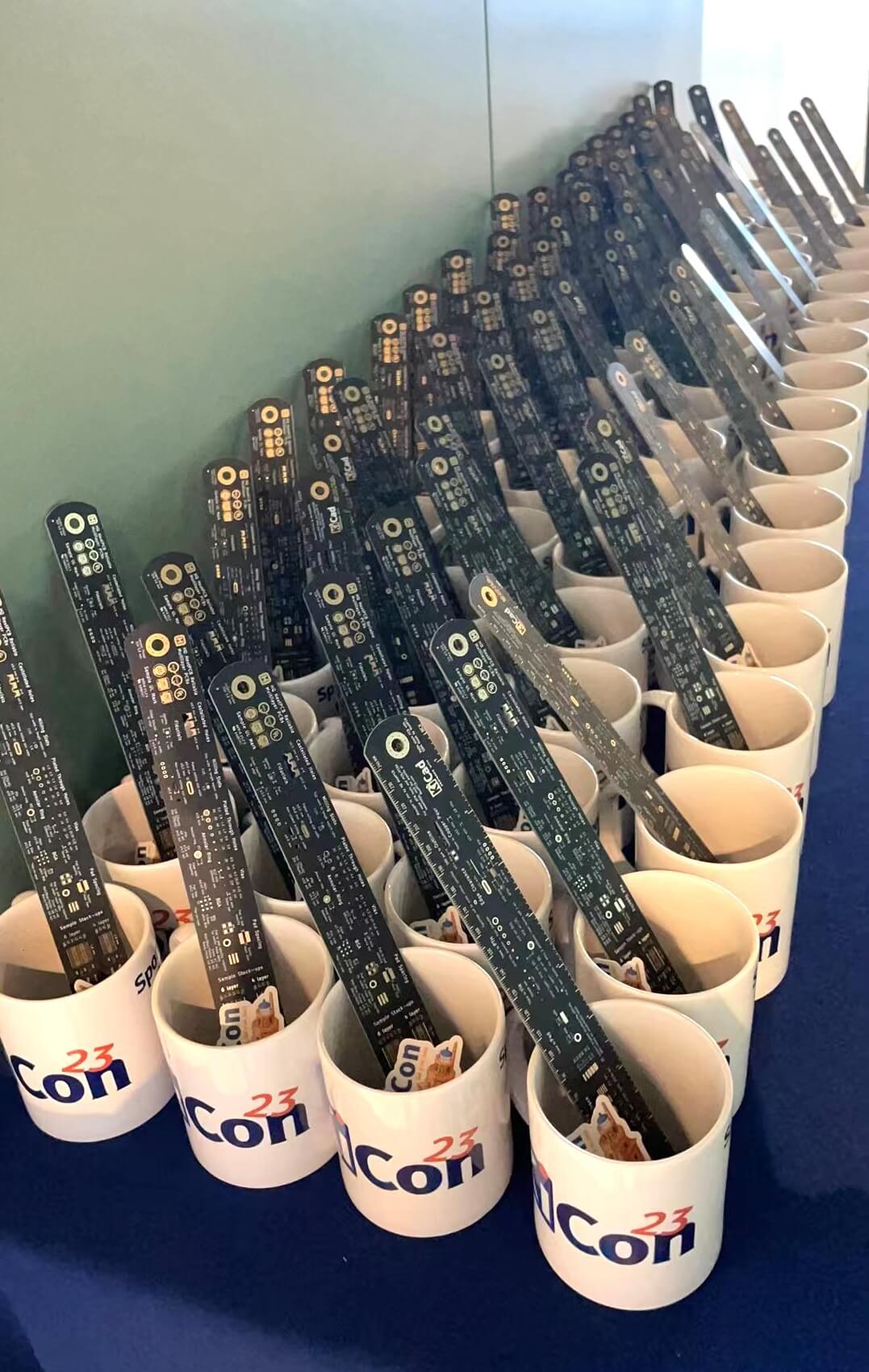
 PCB Assembly
 Layer Buildup
 Online Tools
 PCB Design-Aid & Layout
 Mechanics
 SMD-Stencils
 Quality
 Drills & Throughplating
 Factory & Certificate
 PCB Assembly Factory Show
Certificate
PCB Assembly Factory Show
Certificate
Support Team
Feedback:
support@nextpcb.comWho doesn’t love a good PCB ruler? Few engineers would turn their nose up if handed one at an expo. And it makes for a great branded gift. So when thinking of swag ideas for NextPCB, I jumped at the chance of designing my own ruler.
This post sums up my experience creating the DFM RuleR and tips on how you can create your own, including insider tips from a manufacturing perspective to make sure it comes out as pretty as possible. After working in the Chinese PCB manufacturing industry for over 8 years (and exploiting the free PCBs), I have seen a good share of interesting PCB art techniques, failures and their solutions. The discussions here are geared towards online quickturn PCB services like those offered by NextPCB, JLC and PCBWay because - let’s face it, this is what most of us DIYers can afford.
Many of these tips don’t just apply to rulers. Whatever PCB art you’re making, I am pretty sure you’ll encounter one or two new tips you’ve never heard of.
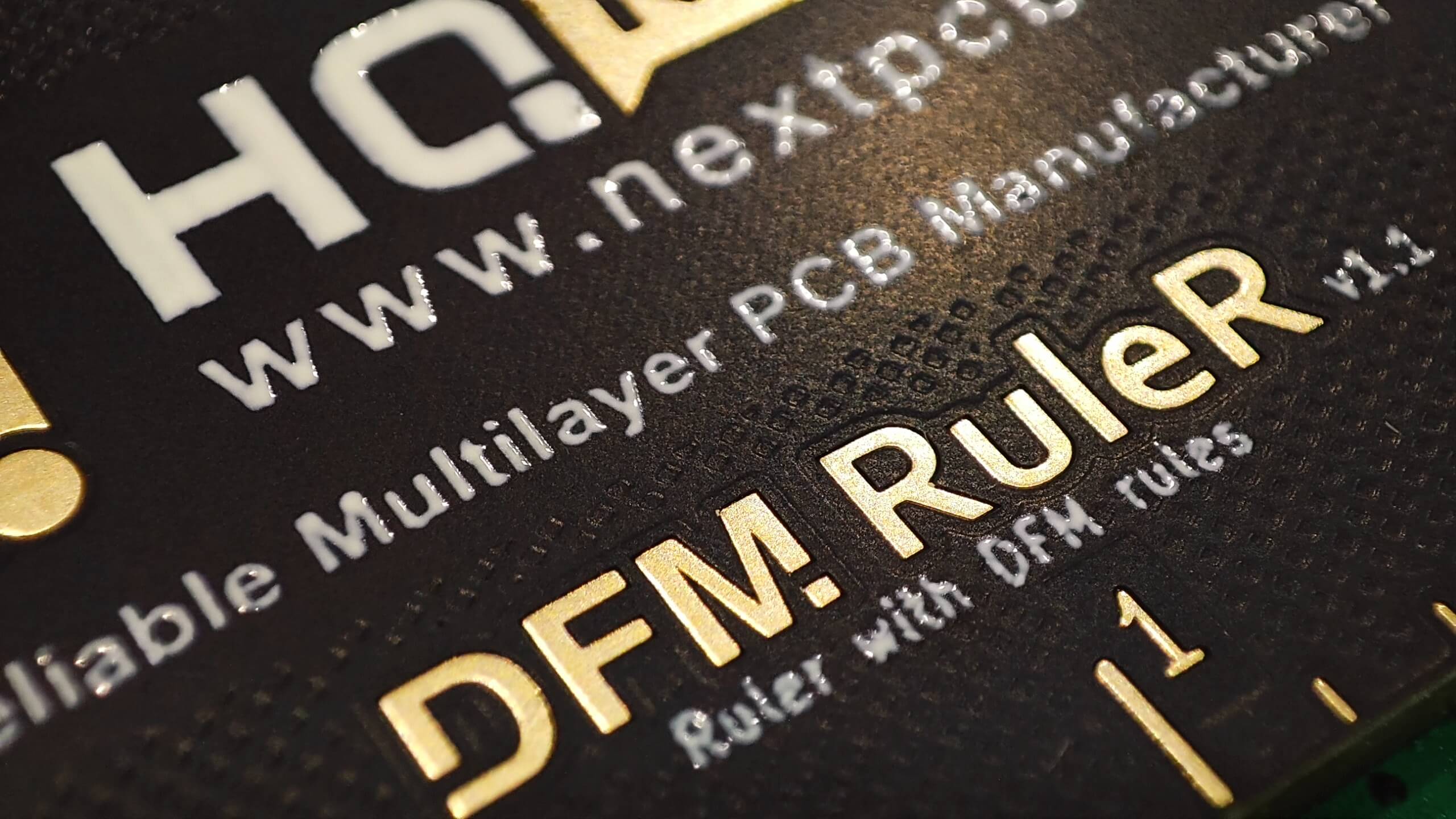
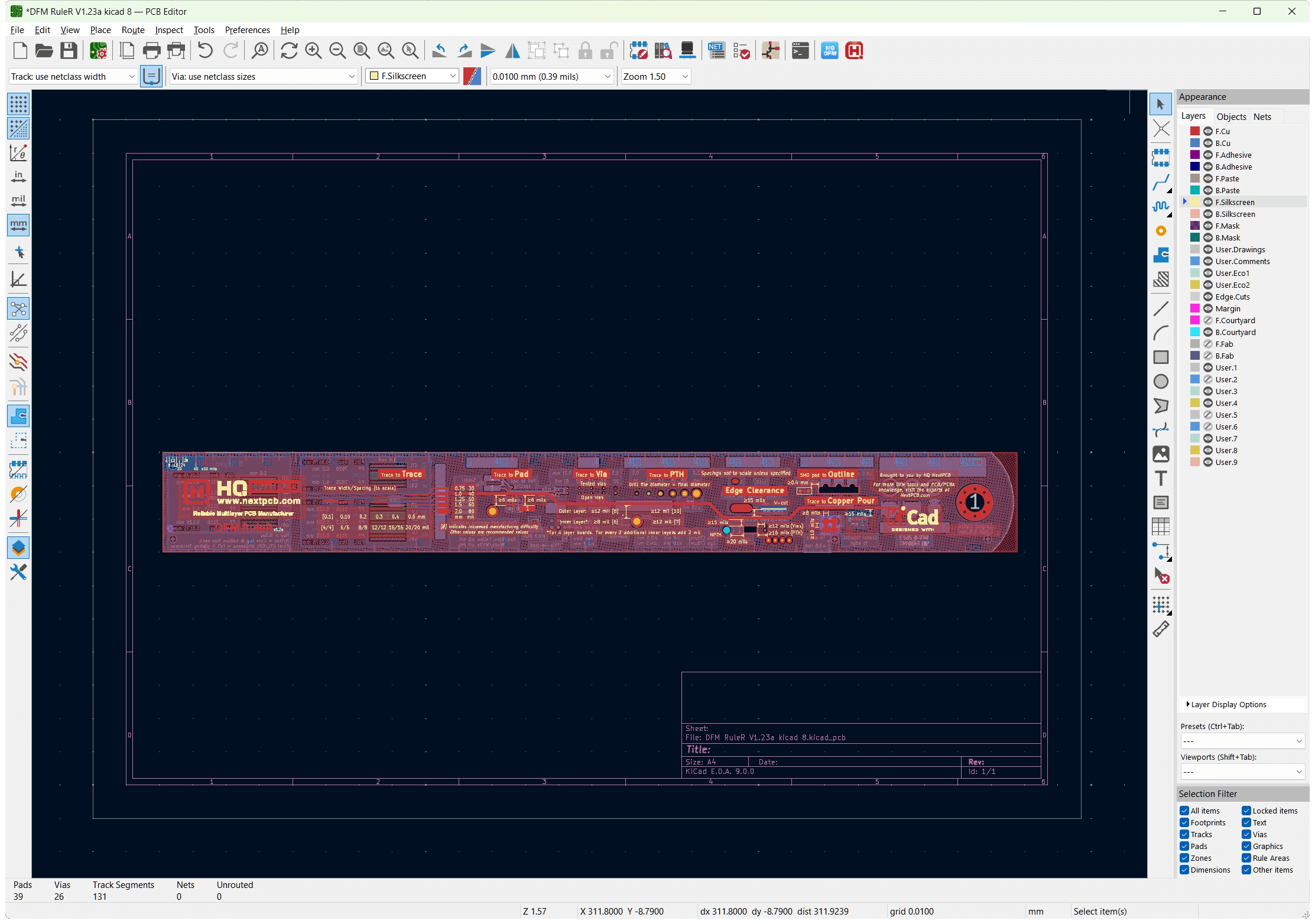
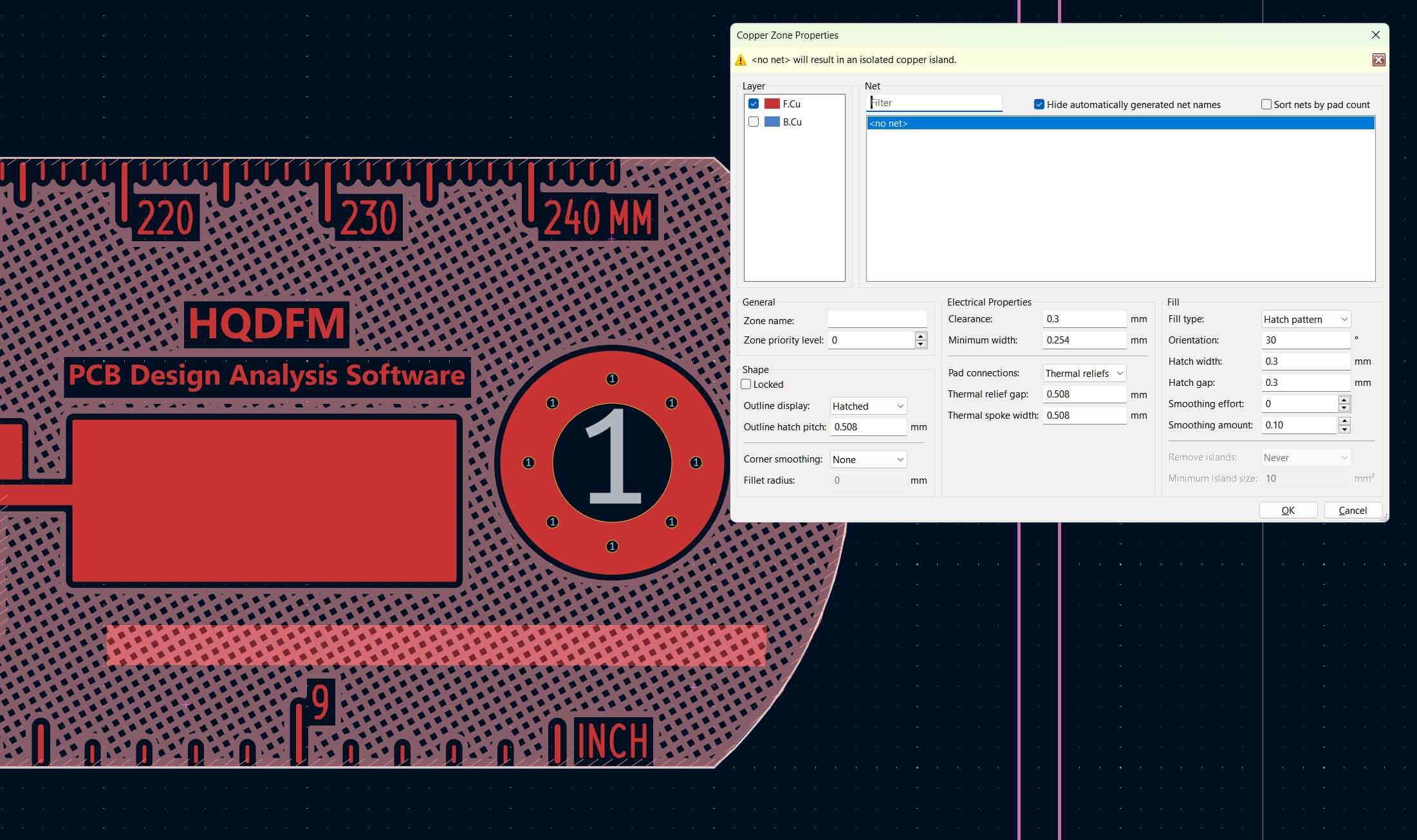
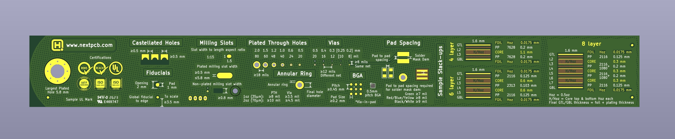
Close-up view of the NextPCB DFM RuleR design with KiCad
KiCad and Gerber files - This is a post about designing your own ruler - go design one. See the appendix for a detailed rant explanation on why this design is not public.
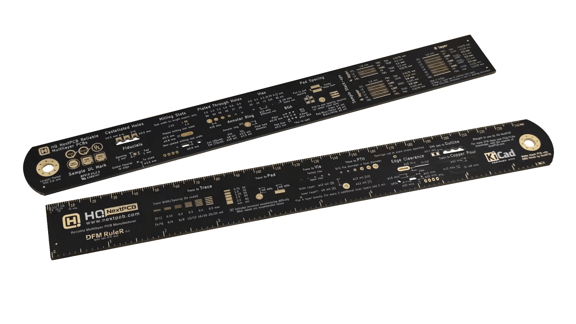
Nowadays, they all look the same except for a change of logo and they’re not all that useful anymore. There are even people selling the standard PCB ruler designs and offering white labeling services. But there are a lot more useful references that engineers could benefit from at hands reach, aside from the standard component footprints and trace widths.
My position here at NextPCB provided the answers. Part of my job is to promote NextPCB’s PCB design analysis software called HQDFM. I had used it even before I came to work for NextPCB in the early days when it pretty much helped transform the industry (in China at least). Before then, I had helped write a DFM booklet that had a ton of specific figures on recommended clearance values and dimensions accompanied by illustrations. It wasn’t just generic stuff like ensure there is sufficient space between the board edge and the trace (how sufficient is sufficient?) and it was stuff recommended by manufacturers who would look at customers’ files all day. They had to decide on these rules, and now they were all available in a little booklet, a booklet that I had on my office desk at all times.
To be fair, looking at my desk now, it seems everything is on my desk at all times, but at least I knew exactly where to dig for it.
It was nice to have a physical reference I could just grab and flip to the folded corner, instead of scrolling through hundreds of bookmarks and tabs looking for the right page - something of a rarity in this day and age. I thought it would be nice to preserve that experience with a PCB ruler with DFM rules and helpful manufacturing related information. Oh and the best part? It’s another excuse to play with KiCad during work hours.
Like many others, KiCad has always been my tool of choice for PCB art. The open-source nature and resident KiCad art fanbase mean there are many tools and workflows available to create some truly breathtaking pieces within the limitations of what is possible on a piece of FR4. A quick Google search will showcase many prime examples of PCB art, most likely made with KiCad in combination with other tools.
Thankfully, this particular design didn’t need any of that fancy work, and unless you intend to add some complex graphics, KiCad’s built-in tools are more than enough to create everything you see on this ruler.
NextPCB also has a close relationship with KiCad beyond the regular $$$ sponsorship, including hosting KiCon Asia which is always a lot of fun. You can even download KiCad from NextPCB's gateway page and get free PCBs for your KiCad design. So with this ruler, I was hitting all my targets with one stone; KiCad, HQDFM, NextPCB.
Before we get started, as with any PCB art project (not the UV inkjet printing stuff), it is important to remember that the fab house likely doesn’t want you doing this! PCBs are printed circuit boards, not printed paperweights, so, as you can imagine, the entire manufacturing and quality management process is tailored to making qUaliFyinG ciRcuIt BoaRds. Standard DRC and DFM rules don’t apply and the technician looking at your files has to make many non-standard decisions on how to approach your design.
Working circuitry might not necessarily be important for your PCB art, and it probably doesn’t matter if solder mask is broken here or there, or an exposed piece of copper is not large enough to test. Likewise, it is unfair to judge a manufacturer’s quality based on these non-standard elements, as you are essentially rewriting the rulebook. Something may look ugly, but it is perfectly allowed under IPC Class 2 (the most common inspection standard). Likewise, a defect that would usually fail quality inspection could pass through because you said just follow the files. It’s entirely subjective.
At the end of the day, they are just aesthetics, so don’t get in a fit if something doesn’t turn out right or the same set of files produces different results (such complaints probably won’t get you anywhere except for a bad relationship with your fab house). The best we can do as artists working on a borrowed medium is to minimize the chances for error in the design, experiment, and try not to over-complicate things.
From the onset, you should have a basic idea of what the final design should look like, especially the color palette. The choice of solder mask color will have a major impact on the range of colors available at your disposal and will influence the overall appearance.
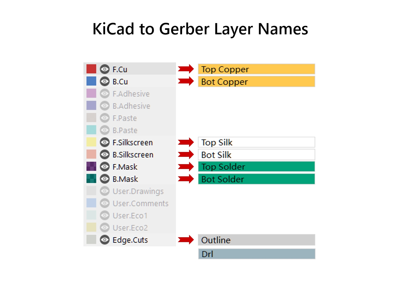
-- If you don’t know what Gerber files, solder mask, silkscreen, surface finish are, I suggest getting familiar with this before diving in. Though the image below pretty much sums it up. Thankfully, the layers in KiCad are very intuitive and pretty much correlate to the Gerber layers that are used for production, with the exception of the drill layer.
Possible PCB art effects
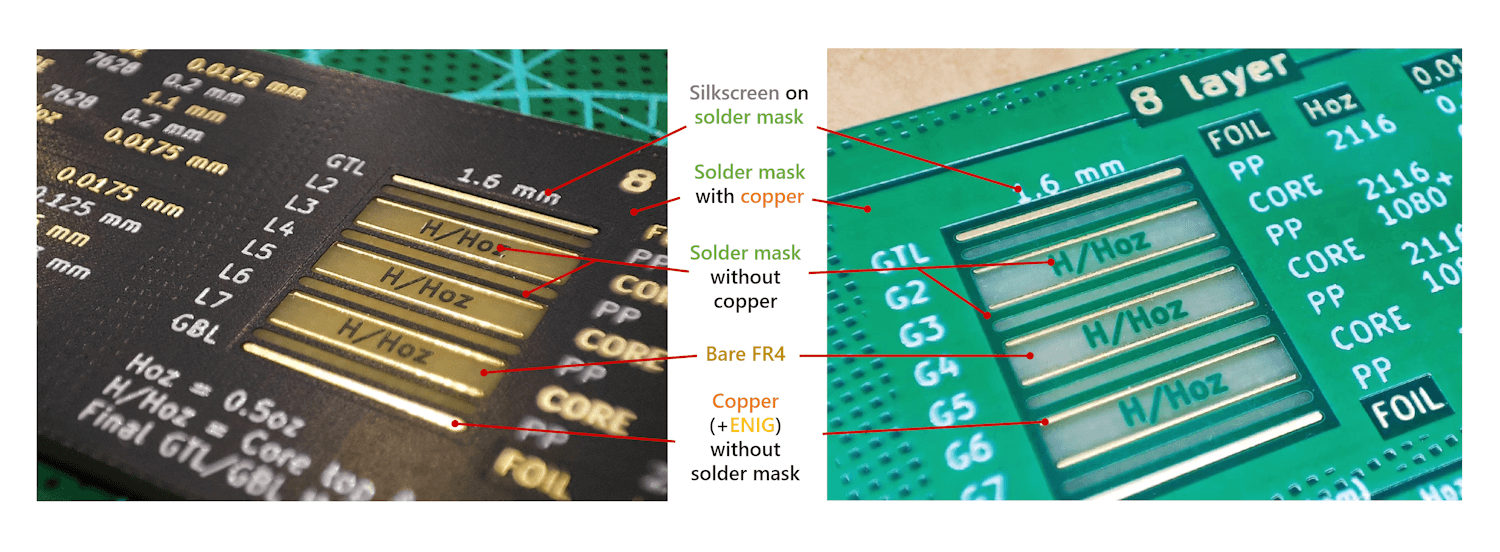
Generally, green and yellow provide a strong contrast between areas with and without copper beneath the solder mask layer, followed by red then blue. White and black on the other hand produce nearly no contrast at all, in exchange for a more subtle embossing effect.
Also, note that the exact color and degree of translucency of solder mask and substrates may vary between manufacturers and even batches. FR4 substrate is slightly translucent, so the appearance of lighter substrates can be influenced by lighting and the color of the surrounding solder mask as is evident in the image above. In strong lighting, you may even see features on the other side of the board, especially with thinner substrates which may be undesirable. However, for a quickturn service, you likely cannot dictate what color FR4 the manufacturer uses so my advice would be to just live with it and accept that there will be variations - oh and don’t get me started on custom solder mask colors.
For this matte black ruler with ENIG surface finish, I only had three colors in my palette:
Oily fingers beware! Matte black is very susceptible to grime - You have been warned.
Personally, I think matte black and ENIG were just meant to be so I am more than happy to give up the extra shade. Bonus - NextPCB doesn’t charge extra for matte black. ENIG, on the other hand, is another story..
With a quickturn service, you really only have two surface finish options - gold (ENIG) or a shiny silver (HASL). The silver shine of HASL surface finishes can look tacky and uneven; however, ENIG surface finish has a layer of real gold, so don’t expect it to come cheap. And if your boards need a lot of gold (large exposed copper surface area), be prepared to pay extra! I intentionally kept the gold surface area below 25% (you can find this value using HQDFM). If you are making a big batch, the costs spread out, so I certainly think it is worth it.
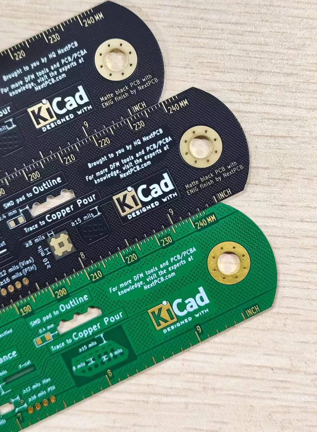
Also, did I mention that ENIG ages like fine wine? The ENIG finish on a board left out in the open has a stronger, darker hue compared to one ripped out of the package, which is almost whitish. In the photo below, the green board on the bottom is a couple of months old, and the top board was just removed from the heat-shrink wrap.
With HASL, the surface will probably just get more grubby and dull as time goes by.
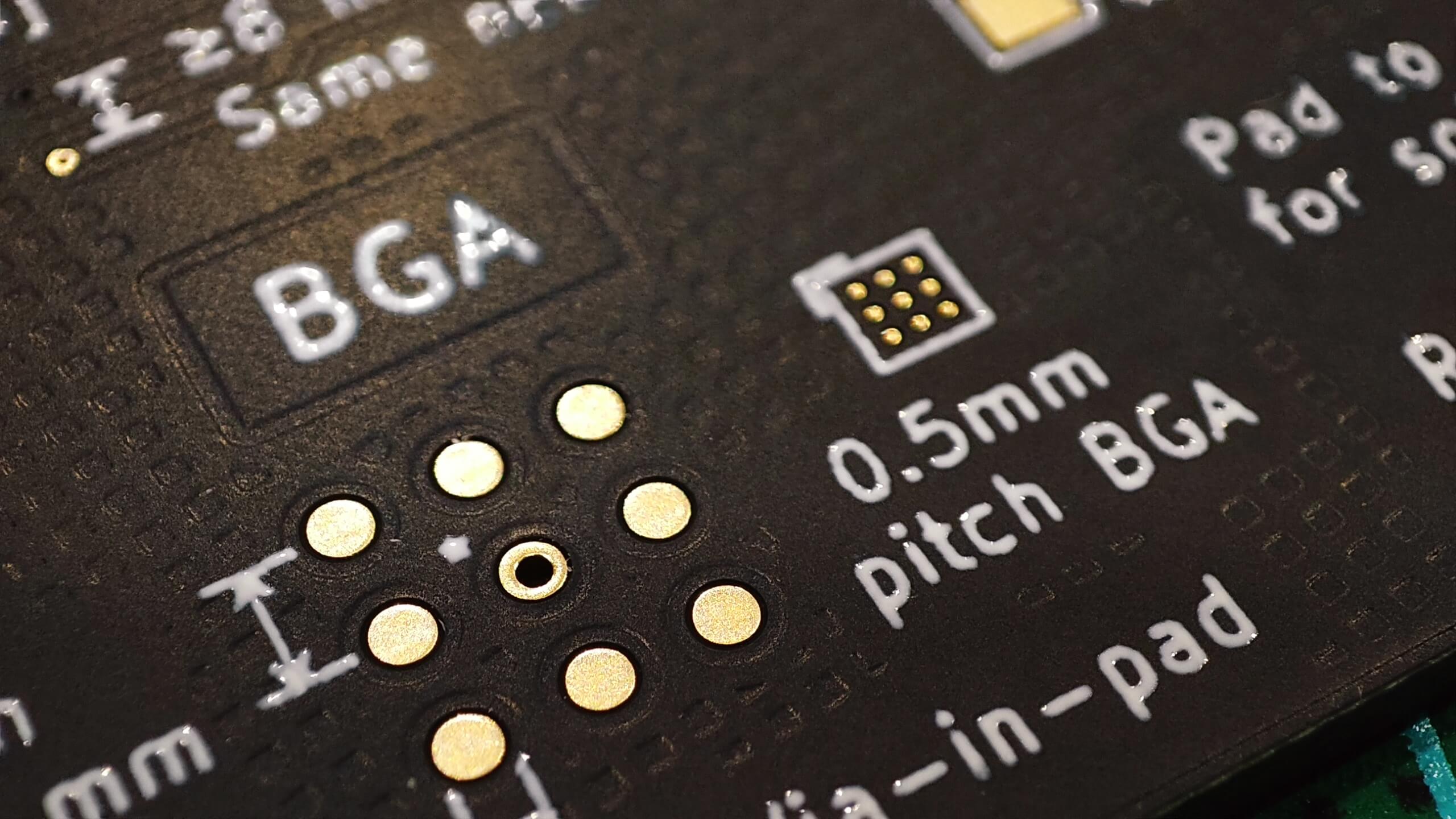
As with any new design you should start with the board outline. You’ll notice this ruler can’t measure the full 30cm like a typical ruler since it has a rounded end, not unlike many stainless steel rulers. Why? ‘Cause it looks fun with the huge golden plated hole in the middle and it decreases the risk of injury when you swing it around like a pendulum. (If someone knows why these mounting holes have vias please let me know)
The curved edge was made using the arc tool then making sure they lined up exactly with the ends of the straight edges. You can make sure they are lined up exactly by entering the same x and y values in the properties window.
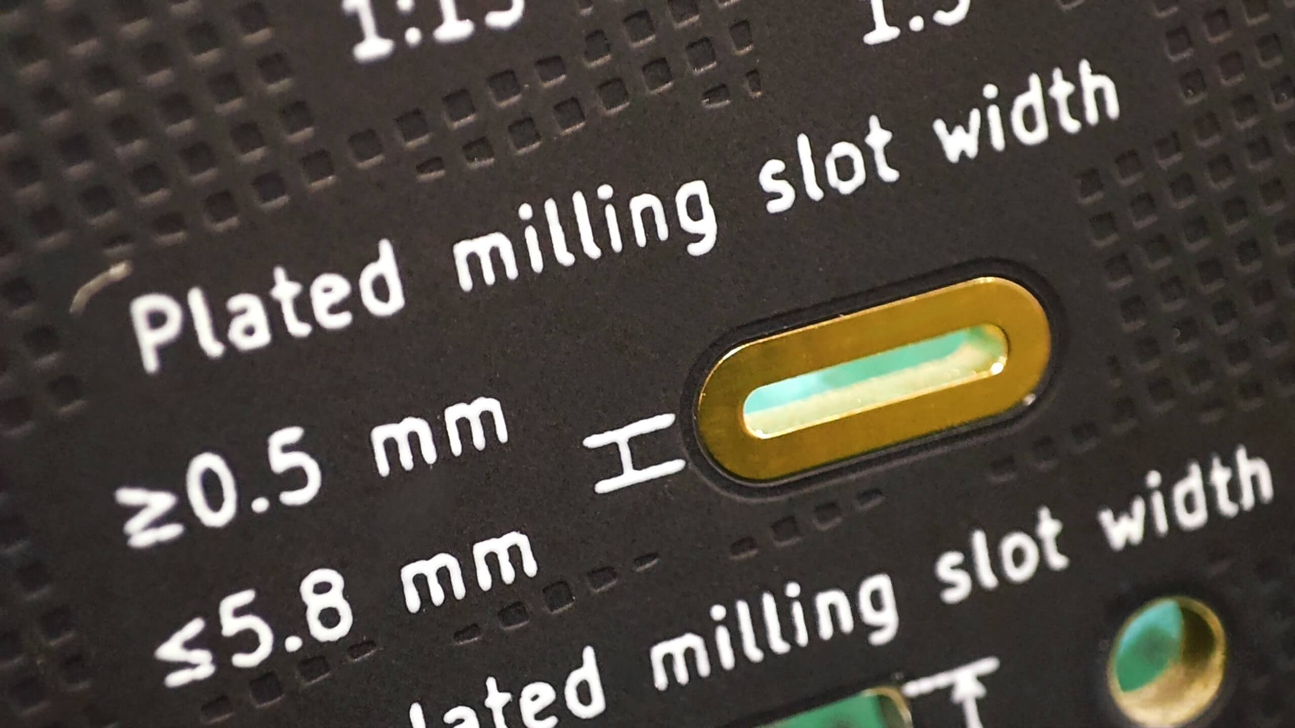
You can also use the outline to add more dimension to your art, in addition to your color palette. But use it sparingly - we are milling out PCBs with a tool bit of 1-2mm diameter, not laser-cutting paper, and too much milling could increase costs. Plated through-hole elements should be limited to small slots and plated drill holes.
And unless you want to file down rough edges yourself and get fibreglass in your eyes, you shouldn’t be panelizing the design. For big batches, be sure to specify singular boards, not a panel for that nice smooth edge.
The ruler uses a cross-hatched copper plane fill for the background pattern. If the grid size is small enough, this produces a subtle raised gradient effect. I find a hatch gap and width of 0.3mm produces just about the right level of gradient without appearing like a hatched copper pour from arm’s length.
Adding a hatched copper pour for a raiseed gradient effect
Playing with a copper pour background is finicky and it can take some time to get the desired effect. For example, the gradient will impact the clarity of fine silkscreen text printed on top. You can get around this by adding a solid copper block underneath. In the NextPCB ruler design, I used a combination of solid blocks in the same net, in different nets and copper voids to make various raised and depressed effects.
All the other features on this ruler were made with KiCad’s basic tools and stock footprints so there is not much to say about these. As said before, keep plated elements small since these are typically are drilled out (not milled). If you need larger plated holes and slots, they will likely incur additional processing costs.
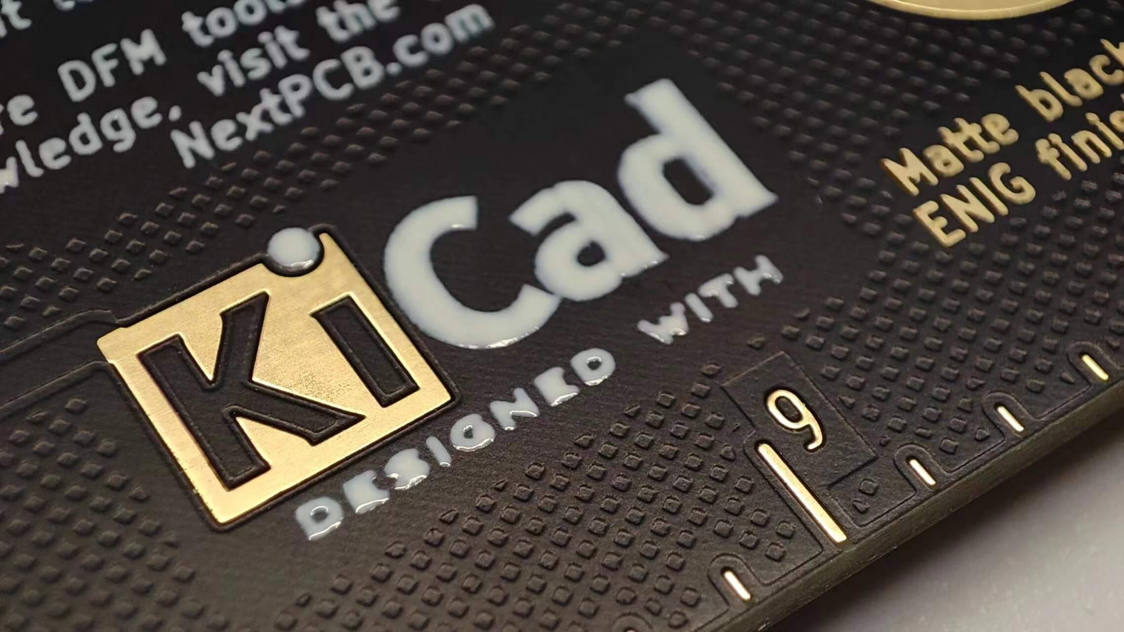
So you are probably going to need some simple graphics on your ruler to make it your own. KiCad’s in-built Image Converter tool is perfect for the job and is very simple to use.
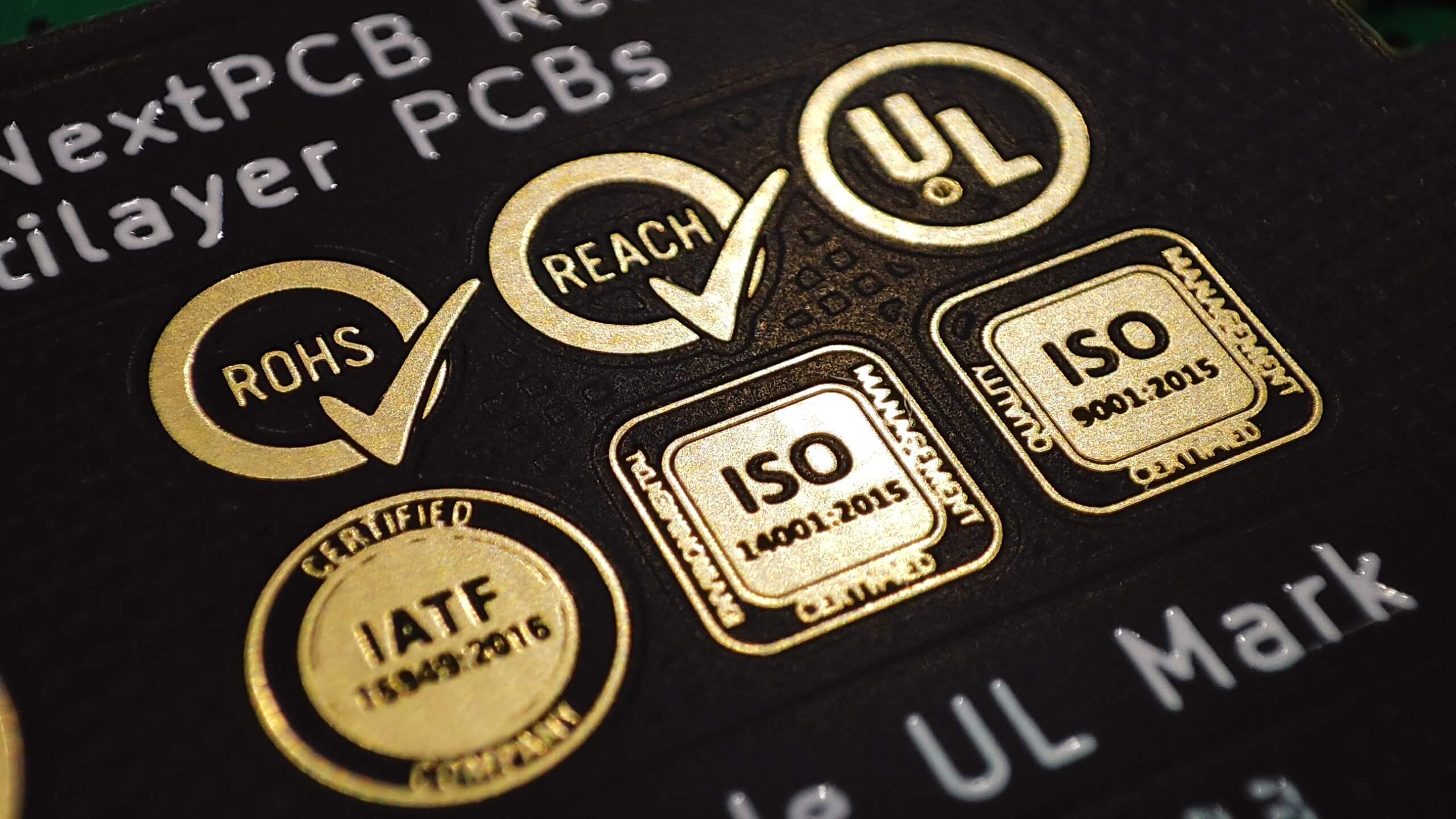
The KiCad Image Converter tool was used to add the main logo and certification logos to the design

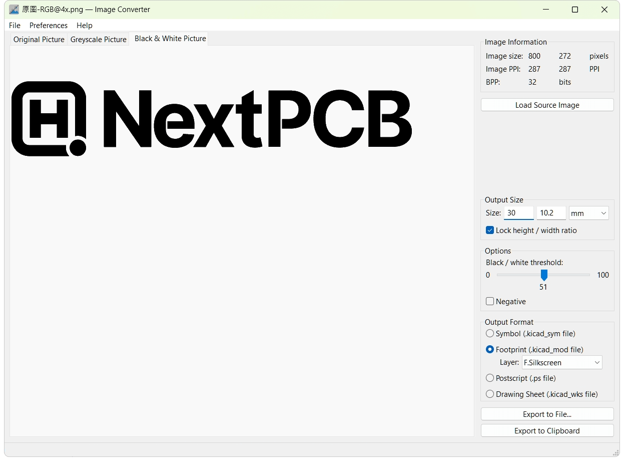
Now, like any other footprint, you can add it to your layout and even edit it in the footprint editor.
Time to produce!
This is the moment you remember that you are borrowing a circuit board fab to make your art.
It is typically standard practice to remove any silkscreen printing present on top of exposed copper areas. Why? Because most of these exposed copper areas are going to be copper pads that required soldering onto in some way. The silkscreen ink will burn with the solder, potentially affecting the quality of the solder joint. Fab houses have automated tools to process Gerber data for production. This includes tools to remove silkscreen on exposed copper or even areas with no solder mask. KiCad even has the option to Subtract solder mask from silkscreen (should that be the other way round?) when exporting Gerber files so you can preview and have better control of the final result. Imagine with one click of the mouse, a huge chunk of silkscreen is deleted from your board without your knowledge.
How to work around this? Here are some solutions:
If you can reliably add notes and get them noticed before production, you might as well add some other, important notes. Some order forms have the option to select these features directly, which is always better than adding it to the notes section.
So it may come as no suprise that this ruler was made by NextPCB. As a NextPCB employee, I’d be told off for not exploiting this opportunity to advertise our services but even before joining NextPCB, most of my art PCBs were made by them and I worked with them even before they were called NextPCB. Quality aside, the two most important features that ensured the boards came as expected were firstly, the ability to add precise notes that will be reviewed and secondly, the option to review working Gerber files. With these two features, you can catch many potential issues beforehand and have much better control over the results.
I have had a number of people ask for the Gerber files of this design and I am all for open-source but after some thought, sharing this particular design doesn’t make sense:
So to stop it from becoming the next ‘standard template’ distributed online with someone else’s logo slapped on it, I have decided not to make the files public. What I can give you however, is a KiCad template with stuff that rulers have like numbers and lines, because that’s what makes a ruler a thing that measures lengths.
Congrats on making it to the end of the article (or did you skip here for the source files?). I hope you enjoyed it as much as I enjoyed writing it. Has it inspired you to go forth and create some of your own PCB art? Have other tips not listed here? Share it in the comment section below.
If you’d like to see more content like this, help me get a one-up on AI content and share it with friends or give me a like.

Still, need help? Contact Us: support@nextpcb.com
Need a PCB or PCBA quote? Quote now


 Printed Circuit Boards
 Surface

