
 PCB Assembly
 Layer Buildup
 Online Tools
 PCB Design-Aid & Layout
 Mechanics
 SMD-Stencils
 Quality
 Drills & Throughplating
 Factory & Certificate
 PCB Assembly Factory Show
Certificate
PCB Assembly Factory Show
Certificate
Support Team
Feedback:
support@nextpcb.comThis ESP32-based board is brimming with an array of sensors, precision circuitry, and a compact design—perfect for running local inference, classification, and decision-making algorithms. Thanks to the dual-core processing power of the ESP32 and its built-in Wi-Fi/Bluetooth connectivity, this board is designed to accelerate the next wave of smart, connected devices. Whether you're building an intelligent home assistant or a precision agricultural monitor, this platform can handle real-time inference, classification, and decision-making right at the edge—no cloud required.
Throughout the design process, I explore the new features of KiCad 9 RC1 and RC2, from schematic creation to layout and preparation for manufacturing, highlighting how these tools streamline PCB development.
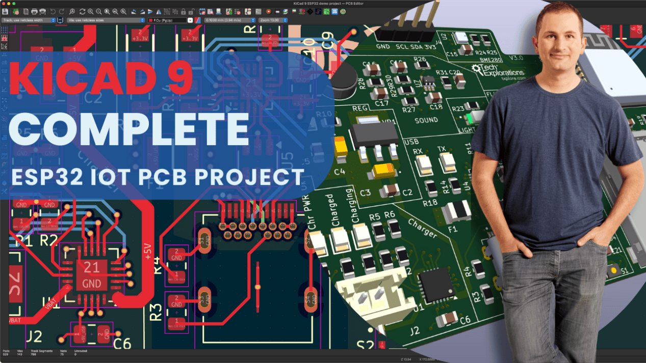
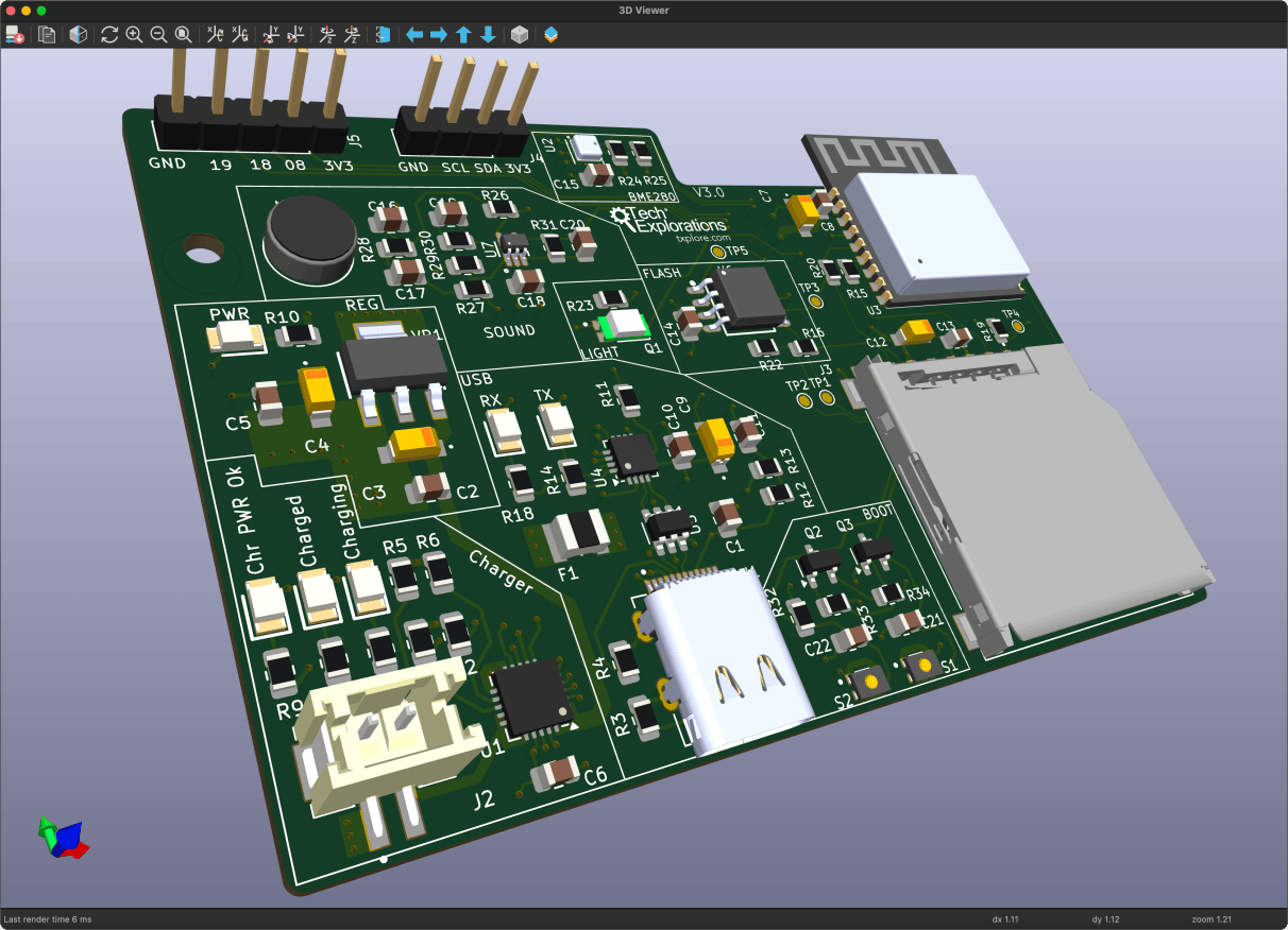
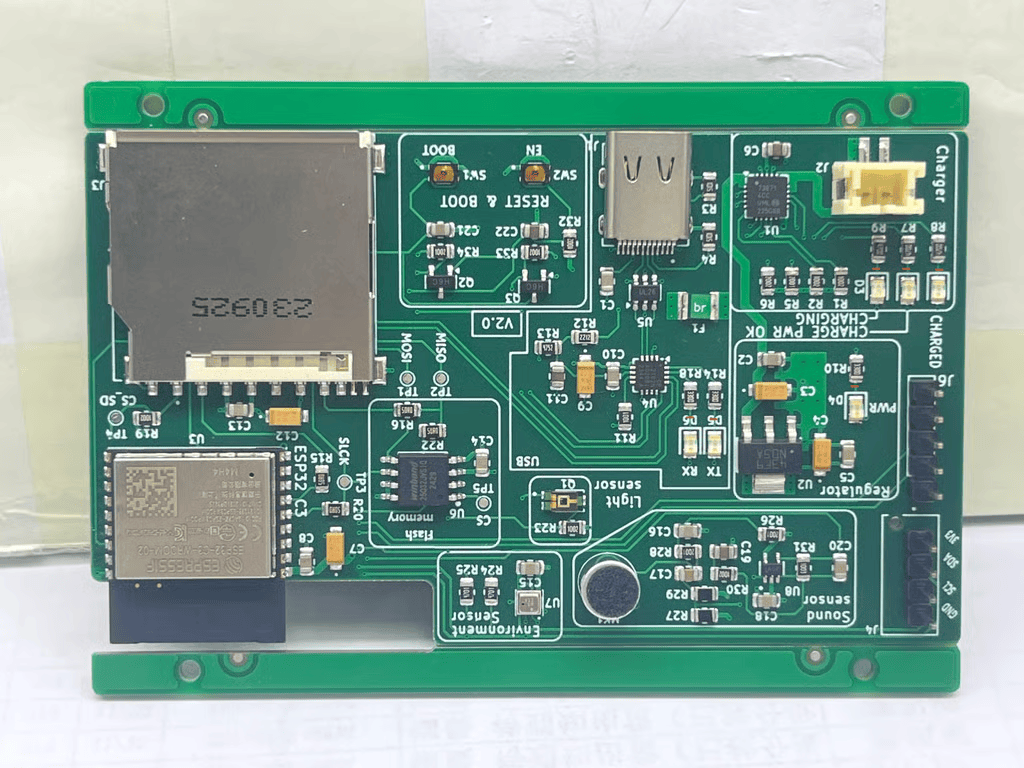
(This 4-layer PCB board is sponsored by NextPCB)
KiCad 9 introduces new features and improvements that significantly enhance its usability, functionality, and performance compared to KiCad 8. These updates cater to schematic and PCB editors and the 3D viewer. The first thing I noticed was how much smoother and faster certain aspects of the workflow were compared to previous versions. Features like the improved routing tools, copper zone management, and the new layer management UI made designing a 4-layer PCB much more intuitive. The interface feels modern and well-organized, which is especially important for complex designs like this IoT board. KiCad can still improve its usability. I’d like to see in the future is greater integration with team-oriented tools like Cadlab and Github.
Want to see these features in action? Follow along as Peter walks through the entire design process—from schematic capture to PCB layout, routing, and fabrication prep—in his detailed tutorial. Some sections are in-depth, but you’re guaranteed to pick up valuable tips!
Learn More: https://techexplorations.com/kicad/kicad-9-designing-a-4-layer-iot-development-board
Youtube Video: https://www.youtube.com/watch?v=LO9AO0XTX3M&t=772s
Still, need help? Contact Us: support@nextpcb.com
Need a PCB or PCBA quote? Quote now
|
Dimensions: (mm) |
|
|
Quantity: (pcs) |
|
|
Layers: 2 |
Thickness: 1.6 mm |
|
|
|

 Printed Circuit Boards
 Surface

