

 Printed Circuit Boards
 Surface
 PCB Assembly
 Layer Buildup
 Online Tools
 PCB Design-Aid & Layout
 Mechanics
 SMD-Stencils
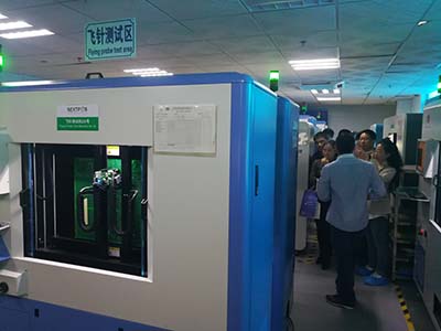
 Quality
 Drills & Throughplating
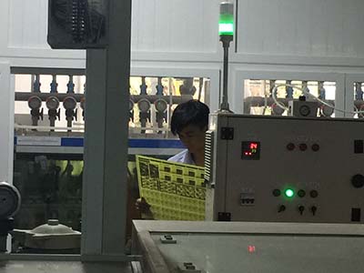
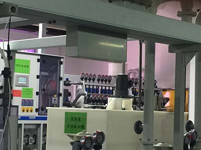
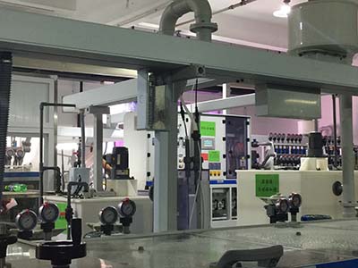
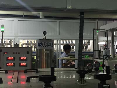
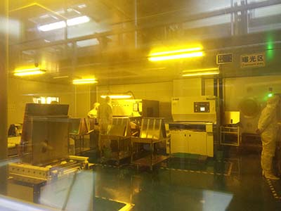
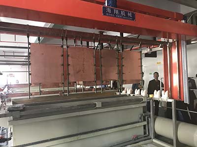
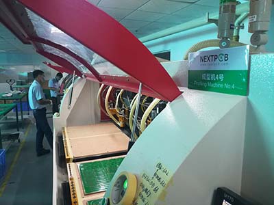
 Factory & Certificate


-
-
-
-
-
Tips and methods for high frequency PCB design
1. The corner of the transmission line should be at a 45° angle to reduce the return loss.
2853 1 0 Shares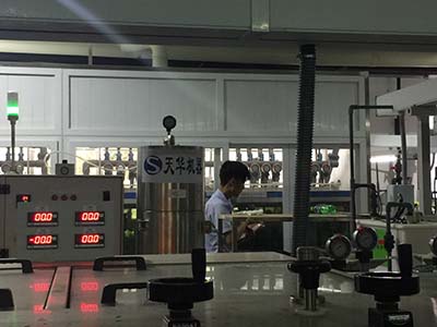
-
Several issues that should be taken seriously by mobile phone PCB design
1. Power and ground processing
3031 1 0 Shares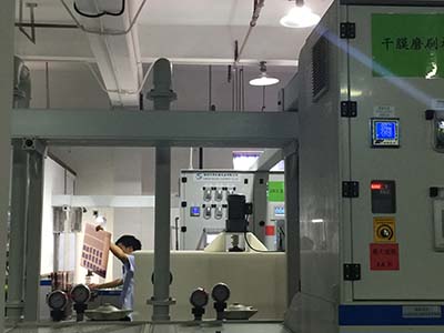
-
How to ensure that no noise is added when designing PCB
It must be considered from the following aspects:
2819 1 0 Shares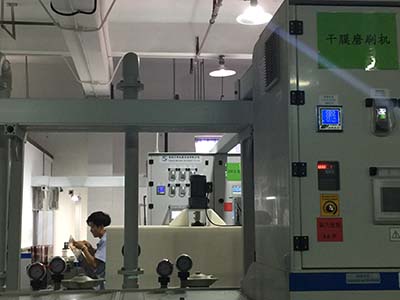
-
RF layout tips for mobile phone PCB design
The increase in the functionality of the mobile phone requires higher design of the PCB.
2841 1 0 Shares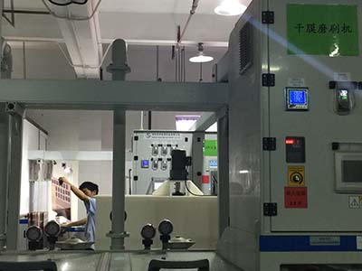
-
PCB design tips 100, teach you to master PCB design easily (25-30)
In this article, we will teach you how to do a PCB design easily 25-30
3025 3 0 Shares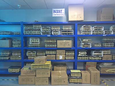
-
-
-
-
-
PCB Design Process - Introduction to DFM
Allow enough test interfaces to facilitate ICT testing
3399 1 0 Shares
-
-
PCB layout and system test
The basic principles of high-speed PCB layout are as follows:
3476 1 0 Shares
-
-
-
-

Categories
Recommended Article:
- Unlock Open-Source FPGA Innovation with Tang Primer 25K from Sipeed - NextPCB Accelerator #8
- Top 9 Most Common IC Packaging Types in Modern Electronics
- Harnessing the SIM7600's Full Potential: A Systems-Level Perspective
- Comprehensive Comparison of PCB Additive and Subtractive Methods
- Deploy Smarter IoT solutions with SIM7600 4G LTE Modules and Free Prototypes - NextPCB Accelerator #7
- Understanding the Differences Between CPU, MCU, MPU, SoC, DSP, ECU, GPU, and FPGA
- RAK3172: The Ultimate LoRaWAN Module for IoT Applications in 2025
- Build Low-Cost FPGA Projects with Tang Nano 20K and Free PCBA Prototypes - NextPCB Accelerator #6
- NextPCB DFM Tool Exclusive Offer: Get a $10 Coupon Every Month!
- Unlocking FPGA Innovation with Tang Nano 20K: Features, Advantages, and Applications
