
 NextPCB Capabilities
Printed Circuit Boards
NextPCB Capabilities
Printed Circuit Boards
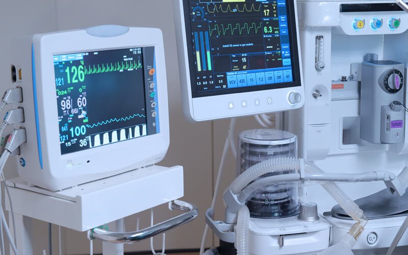
 PCB Assembly
 Layer Buildup
 SMD-Stencils
 PCB Design-Aid & Layout
 Mechanics
 Quality
 Drills & Throughplating
 Factory & Certificate
 PCB Assembly Factory Show
Certificate
PCB Assembly Factory Show
Certificate
Support Team
Feedback:
support@nextpcb.com


SMT, as a common term, has various meanings depending on the context and cultural background. In certain communities or groups, SMT may be used as an abbreviation for specific meanings. For example, on some social platforms, users might create and use unique abbreviations to represent particular concepts, emotions, or behaviors. However, what I want to discuss today is the SMT means in the electronic manufacturing field.

The SMT full form is Surface Mount Technology in the electronic manufacturing field. This is the most common meaning of SMT. It refers to a technique for directly mounting pinless or short-pin electronic components onto the surface of a printed circuit board (PCB), as opposed to the older "Through-Hole Technology" (THT) where leads are inserted into holes. This technology offers advantages such as high production efficiency, a high degree of automation, compact size, lightweight, and high reliability, making it widely used in the manufacturing of modern electronic products. The components used in this process are called SMDs (Surface Mount Devices). This technology is the industry standard because it offers:
The meaning of SMT shifts significantly depending on the industry application, such as the standard SMT process for a toy is vastly different from one required for a pacemaker. A single standardized process can no longer meet the demands for high reliability, special packaging, and adaptability to extreme environments. As electronic products increasingly penetrate fields such as medical, automotive, industrial control, and consumer electronics, different industries have distinct requirements for SMT assembly standards, reliability, cost control, and product consistency. Below, we analyze what SMT means for different sectors.
In the medical field, the definition of a successful SMT process is zero failure. For example, life support systems and diagnostic instruments, demand extreme reliability. Unlike consumer gadgets, a solder joint failure here can be life-threatening. Since products are often used in critical applications like life support systems and diagnostic instruments, there are strict controls over solder quality, component consistency, and board cleanliness, often exceeding those of industrial control products. In actual production, parameters for paste printing, reflow soldering temperature profiles, and electrostatic protection for components must be specially defined. Additionally, because most medical products are produced in small batches but are complex in design, SMT manufacturers need precise process control capabilities and must be equipped with MES systems to ensure traceability throughout the manufacturing process, complying with regulations such as ISO 13485 or FDA standards.
For automotive engineers, SMT quality is defined by the ability to survive harsh physical environments. Vehicle electronic control systems are typically deployed in extreme temperature variations, strong vibrations, and high humidity environments, demanding SMT processes with stronger solder joints and higher environmental adaptability. Common optimization strategies in such projects include using thick copper PCBs to enhance thermal conductivity, employing high-reliability solder materials to resist fatigue from thermal cycling, and applying conformal coating after assembly to further enhance corrosion resistance. Additionally, automotive electronics widely use aging tests and vibration tests, which require systematic and automated quality control systems from SMT manufacturers. Therefore, partners in the automotive field must not only have the necessary equipment capabilities but also be certified under automotive quality systems such as IATF 16949.

Compared to the previous two categories, in industrial controls, SMT balances flexibility with long-term stability. These products are often used in long-running industrial equipment, emphasizing continuous supply and long-term maintenance of circuit boards. Therefore, they often adopt more conservative component selections and more relaxed soldering standards. For example, in some high-reliability industrial controller projects, we frequently encounter customer requests for simultaneous support of both SMT and THT (through-hole technology) mixed assembly, or the need to solder high-power and irregularly shaped components, which poses challenges for flexible line switching and custom fixture capabilities. Additionally, industrial products have long lifecycles with infrequent BOM changes, but the risks of production downtime due to errors are much higher than in consumer electronics. Therefore, contract manufacturers need robust NPI (New Product Introduction) and ECN (Engineering Change Notice) processes to ensure a smooth transition between process validation and mass production.

For consumer products like smartphones and wearables, SMT is driven by market speed and visual perfection. Consumer electronics emphasize cost control and scale efficiency in their SMT requirements, the market is price-sensitive and demands rapid iteration. Additionally, first impressions matter—consumers (and reviewers) inspect the build quality. Thus, the core competitiveness in SMT outsourcing often lies not in the complexity of the processes but in having high-speed and efficient production line resources. For example, the high-density mounting of ultra-miniature components such as 0201 and 01005 requires placement machines to have extremely high positioning accuracy and visual recognition capabilities, while dual-track production lines and automatic loading/unloading systems become key to large-scale production efficiency. Moreover, since consumers place great importance on the "first impression" of products, consumer electronics have higher requirements for board appearance, solder joint uniformity, and clarity of markings. This necessitates that SMT processes are not only efficient but also aesthetically pleasing. Routine inspection processes (such as AOI and SPI) must cover the entire workflow rather than relying on sampling or localized checks.

From the above comparison, it is evident that while the essence of SMT processes is similar, their technical implementations differ significantly in various scenarios. Medical electronics focus on high reliability and fine traceability, automotive electronics emphasize environmental resistance and structural strength, industrial electronics prioritize process customization and long-term stability, while consumer electronics pursue production efficiency and cost reduction. Truly excellent SMT contract manufacturers must flexibly switch between these different demands, execute with precision, and provide integrated process support to customers from product design and prototype validation to mass assembly.
|
Feature |
Medical Electronics |
Automotive Electronics |
Industrial Electronics |
Consumer Electronics |
|
Core Meaning |
Reliability & Safety |
Durability & Resilience |
Stability & Flexibility |
Speed & Cost |
|
Key Standard |
ISO 13485 / FDA |
IATF 16949 |
IPC Class 2/3 |
Cost-Driven |
|
Main Challenge |
Traceability & Cleanliness |
Vibration & Thermal Shock |
High Mix / Low Volume |
Miniaturization (01005) |
|
Inspection |
100% AOI + X-Ray |
Aging & Vibration Tests |
Functional Testing |
Sample / High-Speed AOI |
In modern electronic product manufacturing, SMT (Surface Mount Technology) and DFM (Design for Manufacturability) are two highly related processes. SMT is responsible for efficiently and accurately soldering electronic components onto PCBs (printed circuit boards) using automated equipment, while DFM anticipates and mitigates potential manufacturing issues during the design phase to enhance overall product manufacturability. The collaborative goal of both is to improve production yield, reduce manufacturing costs, and accelerate the cycle from design to mass production.
First, during the component selection and packaging design stage, DFM should align with SMT process capabilities, prioritizing standard package types and ensuring that the packaging library complies with IPC design standards. For high-density assembly boards, it is advisable to avoid using overly small packages (e.g., 01005) or those with narrow process windows to reduce assembly and soldering difficulties. Additionally, in pad design, DFM should recommend appropriate pad sizes, shapes, and spacing based on SMT process characteristics to ensure the accuracy of paste printing and component placement.
Second, in the PCB routing and structural design process, DFM needs to fully consider the SMT production workflow. Routing should avoid placing vias, traces, or copper cutting in assembly areas, as these factors can affect the thermal balance during reflow soldering and may lead to cold joints or warping. For double-sided mounted circuit boards, DFM must also evaluate the impact of reflow process sequencing and thermal stress on components to optimize stacking structures and thermal layouts.
In terms of stencil design and paste printing, controlling solder volume is critical for SMT processes. DFM can provide recommendations for the stencil opening method, shape, and thickness based on component size and pad structure. For QFN or BGA components, it is recommended to use step stencils or fine-tuning openings to avoid solder bridging and voids. These design suggestions typically come from feedback based on SMT production line experiences, so DFM should establish a close communication mechanism with the SMT team.
Furthermore, panel design and component placement orientation are also important aspects of collaboration. DFM should consider panelization methods (such as V-cut or tab routing), fixture space, and placement paths during the design phase to better adapt to SMT production workflows. Standardizing component placement directions not only improves placement speed but also reduces time waste caused by frequent material changes in placement machines.
To better achieve integrated collaboration between design and manufacturing, NextPCB leverages over 15 years of PCB production experience to develop a DFM manufacturability analysis tool, which is freely available to users with no functional limitations. This tool can automatically detect potential manufacturing issues in the early stages of design, helping engineers optimize PCB structures, improve mass production yield, and accelerate the cycle from design to delivery.
In project development, time is critical – and NextPCB delivers. We're your one-stop solution for PCB manufacturing and assembly, turning your designs into reality with speed and precision. From high-quality bare boards to advanced PCB Assembly, NextPCB handles both prototypes and mass production. Our expert DFM support ensures top-tier quality and efficiency. Partner with us to streamline your supply chain and accelerate your projects with reliable, trusted PCB solutions.
Still, need help? Contact Us: support@nextpcb.com
Need a PCB or PCBA quote? Quote now


 Surface

