
 PCB Assembly
 Layer Buildup
 Online Tools
 PCB Design-Aid & Layout
 Mechanics
 SMD-Stencils
 Quality
 Drills & Throughplating
 Factory & Certificate
 PCB Assembly Factory Show
Certificate
PCB Assembly Factory Show
Certificate
Support Team
Feedback:
support@nextpcb.comMost component datasheets include recommended PCB layout information. This recommendation specifies the appropriate hole size for the component, which is the most practical way for PCB hold size selection. However, some datasheets only provide the component's physical dimensions and pin diameter tolerance. In these cases, how should we choose the hole size when creating the component package based solely on these physical dimensions?There is very critical for through-hole component assembly.
Remember this simple rule: Add 0.2mm to the nominal pin diameter for a suitable hole size. Why 0.2mm? Why not just 0.05mm over, or even matching the pin diameter? Component manufacturers apply tolerance ranges to physical dimensions – actual sizes vary from the nominal value (see Figure 1).
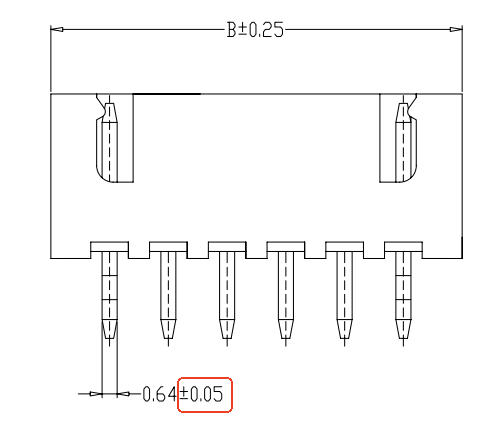
Figure 1
NextPCB encountered this during a customer assembly. The initial PCB batch used holes marginally larger than the nominal pin diameter. While the first assembly succeeded, components failed to insert in the second batch due to pin diameter tolerance stacking.Most pin diameters carry approximately ±0.05mm tolerance. The 0.2mm clearance reliably accommodates this variation, ensuring consistent component insertion.
When selecting via diameter based on pin size, note these critical details:
1. Pin Geometry:
Always check whether datasheet pins are specified as round or square. For square pins (e.g., 0.64mm side length), calculate the effective pin diameter using the Pythagorean theorem.
Example (Figure 2): Diagonal = √(0.64² + 0.64²) = 0.905mm. When PCB layout isn't recommended, design hole diameter = 0.905mm + 0.2mm = 1.1mm.
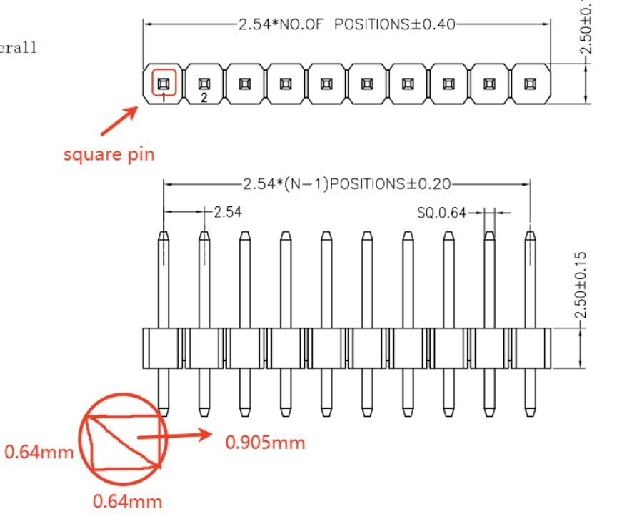
Figure 2
2. One-Sided Tolerances:
If the datasheet specifies only positive tolerance (e.g., 0.9mm +0.1mm/-0), use: Standard value + full positive tolerance.
Example (Figure 3): Hole diameter = 0.9mm + 0.1mm = 1.0mm."
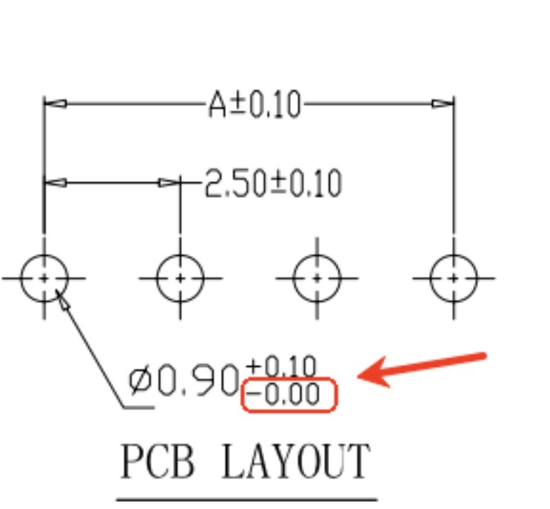
Figure 3
For more knowledge about PCB Assembly, you can try to download our complete PCBA Guide.
NextPCB boasts a dedicated team of over 100 manufacturing engineers solely focused on addressing customers' PCB assembly (PCBA) production issues. We offer comprehensive services ranging from prototypes to mass production. Every PCBA order undergoes rigorous review by our expert manufacturing engineers before manufacturing commences. This approach significantly enhances customer efficiency and prevents over 99% of potential manufacturing problems. If you're seeking a reliable manufacturing partner for your products, NextPCB is definitely your optimal choice.
Still, need help? Contact Us: support@nextpcb.com
Need a PCB or PCBA quote? Quote now
|
Dimensions: (mm) |
|
|
Quantity: (pcs) |
|
|
Layers: 2 |
Thickness: 1.6 mm |
|
|
|

 Printed Circuit Boards
 Surface

