
 PCB Assembly
 Layer Buildup
 Online Tools
 PCB Design-Aid & Layout
 Mechanics
 SMD-Stencils
 Quality
 Drills & Throughplating
 Factory & Certificate
 PCB Assembly Factory Show
Certificate
PCB Assembly Factory Show
Certificate
Support Team
Feedback:
support@nextpcb.comAs we all know, the main factors affecting the delivery time of PCB are the number of layers, impedance, stacking structure, etc. This time I mainly want to introduce the impact of HDI process on delivery time. For example, I recently had a customer whose design had a PCB delivery time of 30 working days. The key reason was that it was a 14-layer HDI third-order board. So, why does the HDI process have such a big impact on the delivery time? Next, I will talk about the HDI production process, how different HDI structures affect the delivery time, and how we can simplify the HDI structure to shorten the lead time.
HDI PCB means High-Density Interconnect Printed Circuit Board. These circuit boards feature a wiring density considerably greater than that of conventional PCBs, facilitated by advanced micro-via and buried via techniques. They are typically employed in miniaturized, high-performance electronic devices.
Extensive information about the production process of ordinary PCBs is already available online, so we will not elaborate here. Our focus is to analyze the core differences between HDI (High-Density Interconnect) circuit boards and traditional PCBs: HDI PCB achieves miniaturization and high performance through precision processes, while ordinary PCBs focus more on basic functions and cost control.
At the process level, HDI PCB adopts laser drilling technology (hole diameter ≤0.1 mm) to replace mechanical drilling, supporting complex micro-hole structures like blind and buried holes, and requires multiple laminations to stack ultra-thin dielectric layers (e.g., below 50 μm) to build high-density interconnects; ordinary PCBs rely on single lamination and through-hole design, with simpler processes. For trace precision, HDI PCB uses Direct Laser Imaging (LDI) and the modified semi-additive process (mSAP) to achieve trace widths/spacings of ≤75 μm, while the etching process for ordinary PCBs only needs to meet the conventional requirement of ≥100 μm.
Regarding materials and fabrication, HDI PCB selects low-roughness copper foil (e.g., RTF) and high-Tg substrates (e.g., FR-4 High Tg) to accommodate high-frequency signal transmission, and ensures micro-hole reliability through electroplating fill technology; ordinary PCBs mostly use standard FR-4 and through-hole electroplating. In the inspection stage, HDI PCB relies on high-precision AOI (Automated Optical Inspection) and flying probe testing to detect micro-defects, while ordinary PCBs can be satisfied with conventional methods.
The divergence in application scenarios is also evident: HDI PCB specializes in fields with stringent space and signal integrity requirements, such as smartphones and 5G communication modules; ordinary PCBs are widely used in conventional electronic products like home appliances and industrial control. In short, HDI PCB exchanges complex processes and high-end materials for ultimate performance, while ordinary PCBs adapt to general needs with cost-effectiveness.
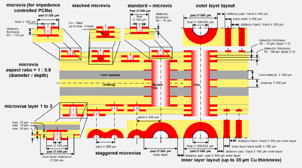
HDI is a special process for producing multi-layer circuit boards with high-density interconnections. It mainly uses blind buried holes and through holes to achieve connections between multiple layers, thereby improving the density and performance of circuit boards, such as supporting shorter signal paths to provide excellent signal integrity, and using thinner dielectric layers and fewer layers to achieve miniaturization and lightweight design. It is generally suitable for multi-layer high-density design, complex signal transmission and space-constrained devices.
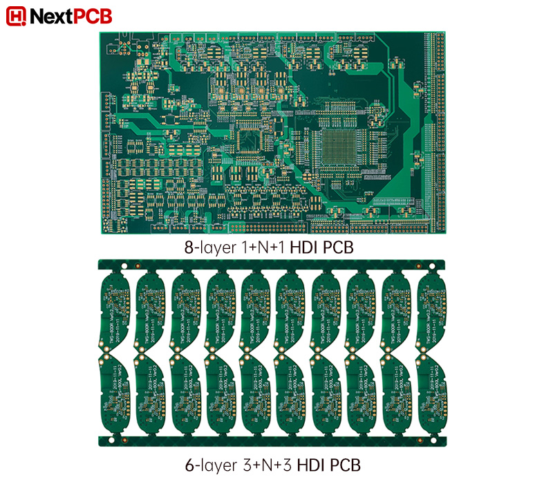
HDI processes are mainly divided into Rank 1, Rank 2 and Rank 3. The main difference is the stacking structure of the lamination and plating cycles. For example, Rank 1 HDI usually refers to the 1+N (number of core layers) + 1 stacking structure of a 4-layer PCB, Rank 2 HDI refers to the 2+N+2 stacking structure of a 6-layer PCB, and Rank 3 HDI refers to the 3+N+3 or 4+N+4 stacking structure of an 8-layer PCB. Among them, different stacking structures correspond to different lamination and plating cycles, such as 2+N+2 requires 3 cycles, and 4+N+4 requires 4 cycles.
Each lamination and plating cycle usually adds 1.5 to 2 days of production time, which directly affects the production lead time. In addition, more lamination and plating cycles will lead to increased alignment errors and defective rate risks, which will increase additional costs to a certain extent. Each lamination and plating cycle requires additional drilling, decontamination and plating steps, which increases the complexity of production. Therefore, if you want to shorten the lead time and reduce costs, it is essential to simplify the stacking structure. Finally, our customer chose to optimize the original 14-layer 4+N+4 to 12-layer 2+N+2 under the advice of our engineers, and replaced the BGA from the blind hole structure to a higher pitch BGA to reduce the need for blind holes. Finally, we successfully compressed the original 30-day lead time to 14 days, reducing costs by 80%. So if you also encounter problems with design requirements, costs, and lead time conflicts, please feel free to contact NextPCB for professional advice and production support!
HDI PCB Quote OnlineNextPCB Stackup and Impedance Calculator
High Density Interconnect: Everything You Need to Know
HDI PCBs: Advantages, Applications and Difficulties in Manufacturing
Still, need help? Contact Us: support@nextpcb.com
Need a PCB or PCBA quote? Quote now
|
Dimensions: (mm) |
|
|
Quantity: (pcs) |
|
|
Layers: 2 |
Thickness: 1.6 mm |
|
|
|

 Printed Circuit Boards
 Surface

