Contact Us
Blog / What is a multilayer PCB?

What is a multilayer PCB?

Posted:09:25 AM December 14, 2023 writer: The Engineering Knowledge

Introduction

PCB boards have now become the main part of the electronic industry. It is considered the main factor in many electronic devices and projects, and different components are assembled on board to make circuits. There are many types of boards, such as single-layer, double-layer, and multiple-layer. Each has its features and design layout and is used for different projects. Multilayer boards come with more than two layers, and their design is an important parameter that needs certain measures to have a good electrical operation and a better signal flow to different components.

There can be different issues, such as signal degradation and noise, that occur if a product is not properly designed or has low-quality materials. A well-structured and accurately configured board comes with accurate functions and signal flow between different layers of the board. Here we will cover different parameters of multilayer boards to get an overview of their importance in industry. Let's get started.

What is a multiplayer PCB?

The type of PCB board is called multilayer PCB, which comes with three or more layers of copper foil that have insulation with each other and are configured in a single unit. In this board, the internal layer core exists in the middle of all layers and is coated with a copper layer from both sides and prepreg used as an insulator. In this board, two external layers are single-sided, and the internal layers are double-sided.

All layers of boards are connected through copper-plated holes, and they can have about forty layers. Active and passive components are connected on these boards' top and bottom layers, and inner layers are used for routing. The multilayer board can handle more components, so it is employed in different electrical projects that need 4 to 12 layers. Different applications, like smart devices, need 4 to 8 layers of boards, and in phones, about 12 layers of boards are used. There are even layer configurations made in these boards since odd layers make complicated structures and expensive boards.

In these boards, for example, the EMI operation signal layer must be configured close to planes and use a larger core between the ground and power planes. The close coupling between signal traces and the ground plane minimizes the crosstalk between traces.

Get Instant PCB Online Quote

How do multilayer PCBs work?

  1. For manufacturing, these boards are made with the use of different PCB design software. After that, the internal layer core is made and laminated with the required thickness of copper foil.
  2. In the next phase, there is a lamination of the board done with the inner layer core, prepreg sheets, and cooper foil sheets.
  3. In this step, with the use of heated hydraulic press pressure, heat and vacuum are applied, and during this process, check that there is no air between layers. Now prepregs connect the sheet, core, and foil to make a multilayer board.
  4. In the design of the board, one layer is used as a ground plane and another as a power plane. For digital boards, a complete power layer is used, and if there is space between the upper and lower layers, it can be used for extra power rail tracks. The power layer exists in the middle of the board, with the ground close to the upper layer.
  5. When power is used by the internal layer, the remaining areas are used for signal routing. For example, there is an eight-layer board with six layers used for signal routing and two for power.

Types of holes in multilayer PCB

A via is an electrical connection between different layers of the board. They are small-sized holes on the board that pass through two or more neighboring layers. Compared to plated-through holes, vias are different. Vias are different since they are used for the electrical connection of through-hole components on board and normally come with a larger dimension than vias.

The via hole is covered with copper to make electrical connections in insulating materials that separate different layers of the board. Based on application needs, boards can need vias that pass through all layers or only the external layer.

There are three main types of vias.

  1. Through-hole Via
  2. Blind Via
  3. Buried Via

Through-hole Via

These vias are commonly used to pass through all layers of the board to connect the upper, inner, and lower layers. It comes with larger dimensions than other vias and can be easily made since there is a simple drilling process.

Blind Via

These vias are made from the external layer of the board to the internal layers and do not make holes on the other side of the board. These vias are called blinds since holes cannot be seen at the sides of the board. During the construction of multilayer boards, certain measures are taken to find certain lengths of holes to the required depth. The main purpose of these vias is to make the connection between the external and internal layers of the board.

Buried Via

These vias make connections between two or more internal layers of the board and cannot be seen through any other outer layer. For multilayer boards, the inner plating of buried vias should be completed before the application of two external layers of the board. Buried vais can increase production costs since they need a high level of accuracy in design.
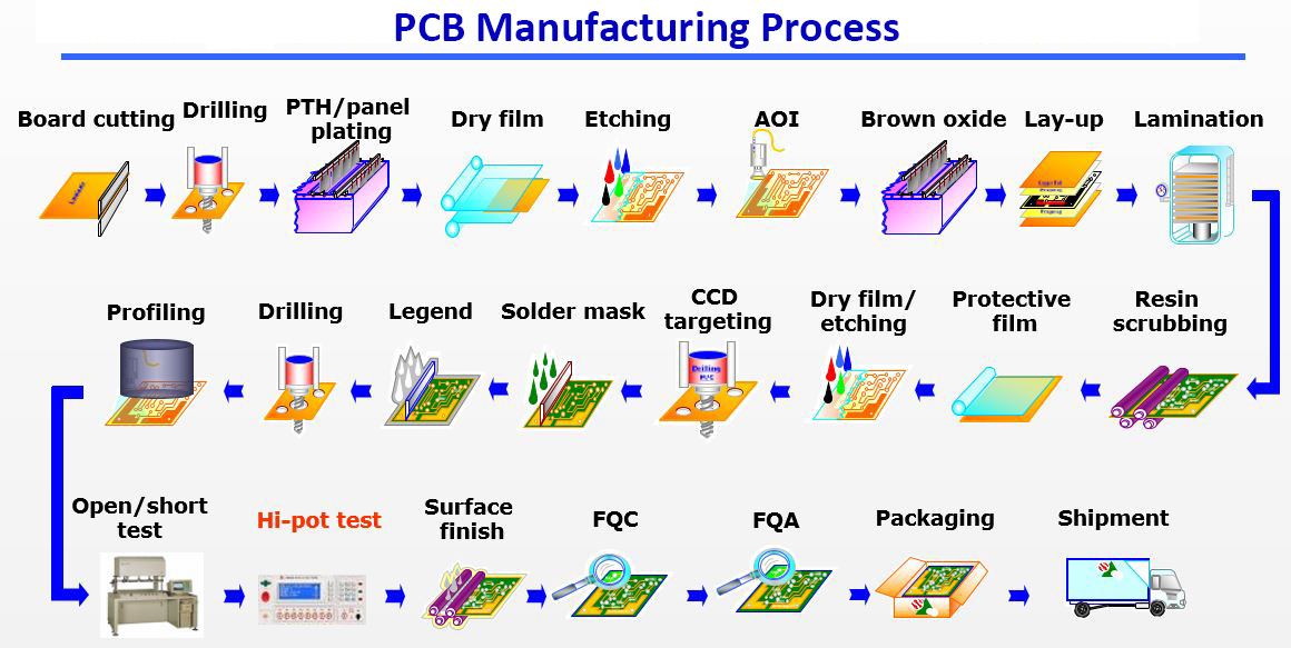
The main production process of multilayer PCB includes

  1. Substrate Preparation: Prepare the base material, typically fiberglass epoxy laminate (FR-4), and cut it into panels of the desired size.
  2. Inner Layer Imaging: Apply a layer of photoresist onto the substrate and use a photo-sensitive film or laser to create the circuit pattern on the inner layers.
  3. Copper Plating: Deposit a thin layer of copper onto the substrate, covering the circuit pattern, through a process called electroplating.
  4. Inner Layer Etching: Remove excess copper using chemical etchants, leaving only the copper traces and pads that form the circuit pattern.
  5. Layer Alignment and Bonding: Align and stack multiple inner layers together, ensuring proper registration of the circuit patterns, and bond them with adhesive under heat and pressure.
  6. Drilling: Drill holes (vias) through the stacked layers at designated locations to establish electrical connections between layers.
  7. Through-Hole Plating: Deposit copper into the drilled vias through electroplating, forming conductive pathways between the layers.
  8. Outer Layer Imaging: Repeat the imaging and etching process for the outer layers to create the circuit patterns.
  9. Surface Finishing: Apply a surface finish, such as HASL (Hot Air Solder Leveling), ENIG (Electroless Nickel Immersion Gold), or OSP (Organic Solderability Preservatives), to protect the copper traces and pads from oxidation and facilitate soldering.
  10. Solder Mask Application: Apply solder mask ink over the entire board, leaving openings for soldering pads and vias.
  11. Silkscreen Printing: Print component designators, logos, and other markings on the PCB surface using silkscreen ink.
  12. Routing and Profiling: Cut the panels into individual PCBs and route any remaining copper traces to final dimensions.
  13. Electrical Testing: Perform electrical tests, such as continuity testing and impedance testing, to verify the integrity and functionality of the finished PCBs.
  14. Final Inspection: Inspect the PCBs for defects, such as shorts, open circuits, and misalignments, before packaging and shipping.


 Multilayer pcb board production schematic

Get Instant PCB Online Quote

Multilayer PCB applications

  1. These boards are used in smartphones, tablets, laptops, and cameras. The compact design helps with the integration of different functions into small-form factors.
  2. These boards are the main components of a computer's motherboard and server system. Their ability to handle complicated circuits and high-speed data transfer makes them the best for use.
  3. It is also part of the router and network infrastructure instruments that use these boards. The high-speed data processing and transmission needed for telecommunication systems are advantages of the design flexibility of boards.
  4. It is used in different medical devices, such as MRI scanners, ultrasound machines, and other medical tools. The feature of integrating complicated circuits into compact designs is important for medical devices.
  5. It is also used in parts of automobiles like engine control units and safety features infotainment systems.
  6. It is also used in aviation and defense instruments that need reliable operation. They are used in radar systems, avionics, and missile guidance systems.
  7. These boards are important for automation systems like PLCs and control panels. Their features for handling complicated control algorithms and interacting with different sensors and actuators are important in industrial settings.
  8. It is also used in routers, switches, and networking cards to speed up data transfer and ensure effective communication in the computer system.
  9. It is also used in power supplies, inverters, and converters due to its ability to handle complicated power distribution circuits and offer effective energy conversion.
  10. The compact nature of these boards allows them to be used in wearable devices like fitness trackers, smartwatches, fitness trackers, and health monitoring devices.

Single Layer vs. Multilayer Layer

Feature

Single-Layer PCB

Multilayer PCB

Layer Configuration

It comes with one conductive layer.

It has many conductive layers configured on top of every layer, with an insulation layer between them.

Complexity

It is less complex due to its one-layer

It is highly complicated due to the larger number of layers.

Design Flexibility

It has limited design flexibility.

High design flexibility can handle complicated circuits and high component density.

Cost

Less cost

High cost than single-layer board due to extra layers and complex manufacturing

Manufacturing Complexity

Its production is simple and easy.

A highly complicated process uses the alignment of layers, lamination etching, and plating steps.

Component Density

Low component density

High component density is best for densely populated circuits.

Signal Integrity

Signal quality losses due to limited shielding

Increased signal quality decreases interference between components.

Applications

Used in simple circuits that are used for basic functions in devices

used in applications like advanced functionality, high-performance electronics, and miniaturization.

Size and Weight

High weight and larger size

Small size and lightweight due to handling components on multilayer

Common Use

Toys, low-cost products

telecommunications equipment, high-end electronics, computers, and medical devices

Multilayer PCBs: Drawbacks

There are some limitations to these boards, like the fact that you must consider the cost of your project before using a multilayer board. Since these boards are expensive, They are not preferred for short-term projects because their manufacturing time is high compared to other boards. Its repair is also a complicated process compared to single-layer boards.

Conclusion

Multilayer boards are becoming an important and main part of electronics. They also have limitations, like high production costs and design complications, with advantages such as high density and less weight. The features of the board handle complicated circuit design and offer a high-level operation that helps to use them in computers, telecom, medical devices, consumer electronics, the aviation industry, and other wearable technology.

The contact form factor, signal quality, and ability to handle complicated functions make these boards important for different devices and systems. Despite the difficulties involved in these board designs and production, the advantages of functionality, reliability, and high space cover their disadvantages.


You may also be interested in...

The better the layer stack design, the higher level the PCB design

Christmas Offer: Get $30 off PCB orders over $100 with NextPCB

New Special PCB Pricing and Low-Cost Shipping Faster than China Post

Free PCB Assembly Offer is Now Live: Experience Reliable PCB Assembly from HQ NextPCB

HQ NextPCB Introduces New PCB Gerber Viewer: HQDFM Online Lite Edition

  • PCB
    Prototype
  • PCB
    Assembly
  • SMD
    Stencil

Dimensions: (mm)

×

Quantity: (pcs)

5
5
10
15
20
25
30
40
50
75
100
120
150
200
250
300
350
400
450
500
600
700
800
900
1000
1500
2000
2500
3000
3500
4000
4500
5000
5500
6000
6500
7000
7500
8000
9000
10000

Other Quantities:(quantity*length*width is greater than 10㎡)

OK

Layers:

Thickness:

Quote now