

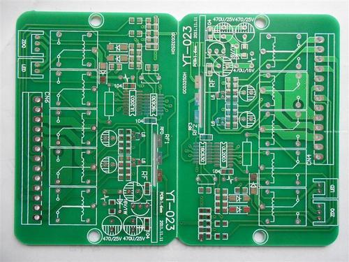
 Printed Circuit Boards
 Surface
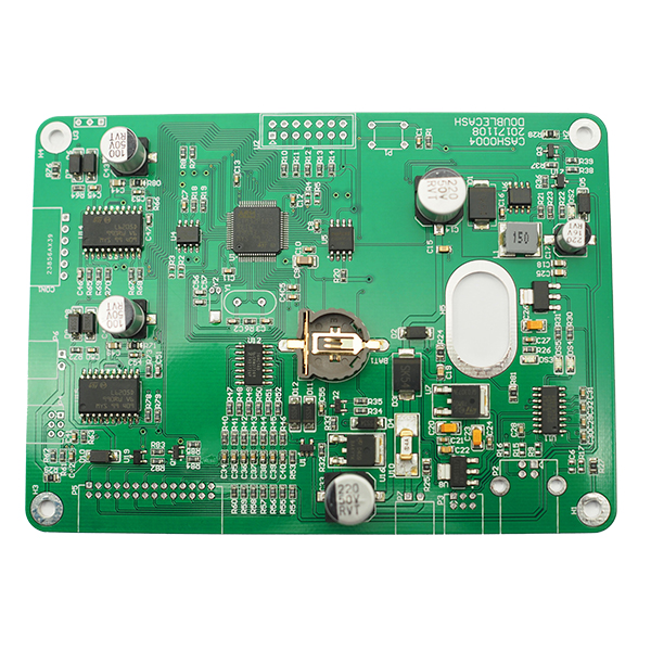
 PCB Assembly
 Layer Buildup
 Online Tools
 PCB Design-Aid & Layout
 Mechanics
 SMD-Stencils
 Quality
 Drills & Throughplating
 Factory & Certificate


In the electronics manufacturing industry, the cost of custom PCBs (Printed Circuit Board) and PCBA (Printed Circuit Board Assembly) has always been a focal point for hardware developers, engineers, PCB designers, PCB manufacturers, and PCB procurement professionals. Whether for PCB prototype or mass production, understanding the factors that impact PCB/PCBA cost will help optimize design, reduce expenses, and ensure timely delivery. This article delves into the various factors influencing the cost of custom PCB and PCBA and offers practical suggestions for reducing customization costs, helping businesses achieve higher returns on investment.
Table of Contents
What is the Difference Between PCB and PCBA
Before discussing the cost of customization, it’s important to understand the difference between PCB and PCBA.
- PCB: A bare PCB board made of insulating materials with conductive traces that provide mechanical support and electrical connection for electronic components.
- PCBA: An assembled PCB, where all necessary components are soldered or mounted onto the PCB, forming a functional circuit.
How much does a custom pcb or PCBA cost?
When it comes to customization, PCB costs primarily involve materials and manufacturing processes, while PCBA costs also include component selection, procurement, assembly, and soldering techniques. For PCB prototypes, prices generally range from a few dollars to several dozen dollars, depending on the complexity and material choices. PCBA prototypes, on the other hand, usually range from tens to thousands of dollars, as they also factor in component costs and assembly processes. To fully understand the cost of customization, it is necessary to discuss the components of PCB and PCBA separately.What Factors Affect the Cost of Custom PCBs
Many people may wonder why custom PCBs are so expensive. In fact, this is due to a combination of several factors. The production of PCBs requires not only high-precision manufacturing processes but also consideration of the materials used, design complexity, production scale, lead time requirements, and strict testing and quality control. Each of these factors significantly impacts the final cost. Understanding these elements is crucial for accurately estimating and managing PCB costs. Let’s explore the key factors that influence the cost of custom PCBs:
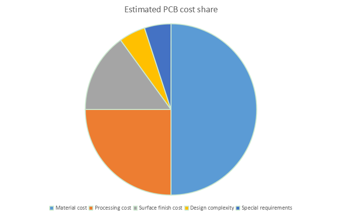
PCB Cost Estimate Breakdown (For Reference Only)
1. PCB Material Selection
How does material selection affect the PCB cost? PCB Material selection is one of the most important factors influencing the overall cost of a PCB. Different PCB materials offer various performance characteristics, and choosing the right one can significantly affect the final price. Common PCB materials include:
FR-4: The most commonly used material, FR-4 is relatively inexpensive and suitable for most general-purpose circuit boards. FR-4 materials come with different TG (glass transition temperature) values, chosen according to the product's thermal requirements.
- Standard TG value (130°C - 140°C): Economical and suitable for standard consumer electronics.
- Mid TG value (150°C - 160°C): Suitable for applications in moderate temperature environments, such as automotive electronics.
- High TG value (170°C and above): Used for devices requiring high thermal stability, such as communication, server, and aerospace products.
As the TG value increases, the cost of the material and the complexity of the manufacturing process also rise, leading to a higher overall PCB price.
| TG Value | 130℃ -140℃ | 150℃ -160℃ | 170℃ -180℃ |
| 2 Layer Custom PCB Cost | $5.00 | $22.14 | $26.57 |
| 4 Layer Custom PCB Cost | $13.00 | $45.13 | $49.56 |
| 6 Layer Custom PCB Cost | $93.85 | $69.00 | $100.60 |
| 8 Layer Custom PCB Cost | $129.52 | 129.52 | $135.82 |
Impact of TG Value on PCB Cost for 100x100mm, 5pcs
High-Frequency Materials: Such as Rogers materials, used for high-speed communication or RF applications, are more expensive. Rogers materials come in various types to meet different frequency and performance requirements.
- Rogers 4000 Series: Suitable for mid-frequency applications, relatively lower in cost.
- Rogers 3000 Series: Offers low dielectric loss, suitable for high-frequency and microwave applications.
- Rogers 6000/RO3000 Series: Used for extremely high-frequency applications, widely used in satellite communication and radar, with stable performance but significantly higher costs.
The better the material performance, the higher the cost and complexity of the manufacturing process.
Metal-Based Materials: Such as aluminum substrates, commonly used in LED lighting and high-power devices due to their superior heat dissipation. Aluminum substrates come in various grades depending on thermal conductivity.
- Low Thermal Conductivity (1.0-2.0 W/mK): Suitable for medium-to-low power applications, such as general LED lighting.
- Medium Thermal Conductivity (2.0-3.0 W/mK): Suitable for mid-to-high power devices.
- High Thermal Conductivity (≥3.0 W/mK): Used for high-power density applications, such as power electronics and automotive lighting.
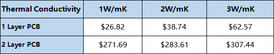
Impact of Thermal Conductivity on PCB Cost for 100x100mm, 5pcs
These high thermal conductivity materials are more costly and have more complex manufacturing processes, leading to higher overall PCB prices.
PCB Cost Impact: Higher performance materials generally mean higher costs. When selecting materials, it is important to balance electrical performance requirements with the budget.
2. PCB Layers
The more layers a PCB has, the more complex the manufacturing process. The cost difference between single-layer, double-layer, and multi-layer pcb boards is significant.
- Single-layer PCB: Basic PCB structure suitable for simple circuits.
- Double-layer PCB: Suitable for slightly more complex circuit designs.
- Multi-layer PCB: Used in more complex designs, especially in high-density integrated electronic devices.
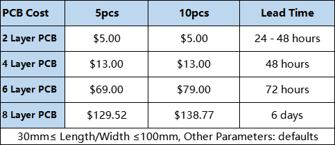
Impact of PCB Layers on PCB Cost
PCB Cost Impact: Multi-layer boards not only require more materials but also involve more complex manufacturing processes, resulting in significantly higher costs compared to single and double-layer boards.
3. Size and Design Complexity
Larger PCBs require more materials, and the more complex the circuit layout, the higher the production cost. If the design involves fine traces, narrow spacing, or micro-vias, it will increase the difficulty and cost of manufacturing. Similarly, smaller PCBs can also lead to higher costs. For example, if the size is smaller than 10mmx10mm(i.e., either the length or the width is less than 10mm), this can increase the production difficulty, thus raising the cost as well. This is due to the challenges involved in manufacturing small-sized PCBs, which typically require more precise processes and specialized techniques.
PCB Cost Impact: Complex designs require more time, technology, and resources to manufacture, leading to higher overall expenses.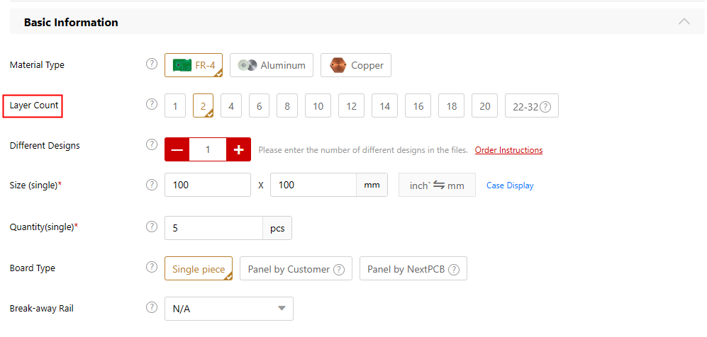
NextPCB supports the production of up to 32 layers of PCB boards
4. PCB Thickness
PCB thickness refers to the overall thickness of the circuit board.
- Standard PCB Thickness: 1.6mm (62mil) is standard and suitable for most applications.
- Non-standard PCB Thickness: Includes options like 0.8mm and 2.0mm, which cater to specific application requirements.
PCB Cost Impact: Increasing PCB thickness can enhance mechanical strength and electrical performance but also raises material costs and manufacturing difficulty. Custom thicknesses may require special manufacturing processes, further increasing costs.
5. Solder Mask Color
The solder mask is a protective layer on the PCB, and solder mask color refers to its hue.
- Green: The most common color, typically cost-effective.
- Other Colors: Such as white, yellow, red, blue, black and matte black can be produced but may increase production steps and slightly raise costs.

PCB Cost Impact: Solder mask color does not directly affect electrical performance but can impact production costs. Non-standard colors may increase material and processing costs.
6. Trace Width and Spacing
Trace width is the width of the conductive paths on the PCB, while spacing is the minimum distance between conductive paths.
- Default Values: Typically 6/6mil. Friendly Reminder: In some cases, the price generated by online PCB quote tools can be higher due to the smallest trace width and spacing requirements. If your design can be adequately supported with 6/6 mil, you can adjust to 6/6mil or larger to help reduce your PCB manufacturing costs.
| Trace Width/Spacing | 3.5/.35mil | 4/4mil | 5/5mil | 6/6mil | 8/8mil | 10/10mil |
| 2 Layer PCB Cost | - | $30.68 | $5.00 | $5.00 | $5.00 | $5.00 |
| 4 Layer PCB Cost | $40.70 | $40.70 | $13.00 | $13.00 | $13.00 | $13.00 |
| 6 Layer PCB Cost | $69.00 | $69.00 | $69.00 | $69.00 | $69.00 | $69.00 |
| 8 Layer PCB Cost | $129.52 | $129.52 | $129.52 | $129.52 | $129.52 | $129.52 |
| 30mm ≤ Length/Width ≤ 100mm. Other Parameters: defaults | ||||||
Impact of Track Width and Spacing Value on PCB Cost for 100x100mm, 5pcs
PCB Cost Impact: Smaller trace widths and spacings require higher manufacturing precision, potentially increasing production costs. Wider trace and larger spacings reduce manufacturing complexity but may not be suitable for high-density designs.
7. Copper Thickness
Copper thickness refers to the thickness of the copper layer on the PCB, usually measured in ounces (oz).
- 1 oz: Common for standard applications, suitable for most circuit board designs.
- 2 oz or thicker: Used for applications requiring higher current-carrying capacity or enhanced heat dissipation, such as power circuits.
| PCB Copper Thickness | 1 oz | 1.5 oz | 2 oz |
|---|---|---|---|
| 2 Layer PCB Cost | $5.00 | $71.28 | $60.94 |
| 4 Layer PCB Cost | $13.00 | $51.88 | $84.99 |
| 6 Layer PCB Cost | $69.00 | $105.03 | $137.08 |
| 8 Layer PCB Cost | $129.52 | $139.95 | $169.87 |
| 30mm ≤ Length/Width ≤ 100mm. Other Parameters: defaults | |||
Impact of Copper Thickness Value on PCB Cost for 100x100mm, 5pcs
PCB Cost Impact: Thicker copper layers increase material costs and processing difficulty but support higher current and better heat dissipation, raising overall PCB production costs. For example, 1oz copper thickness is relatively inexpensive, while 2oz or thicker copper layers require more copper material, resulting in higher raw material costs. Therefore, when designing custom PCBs, it is essential to select the copper thickness based on the actual application requirements, ensuring that performance needs are met while effectively controlling costs.
8. Minimum Drill Hole Diameter
Minimum drill hole diameter is the smallest diameter of holes drilled into the PCB.
- Smaller Diameters: Require finer drill bits and higher processing precision, increasing production difficulty and costs. Common in high-density designs.
- Larger Diameters: Simpler to process and lower in cost but may limit design complexity.
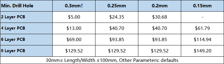
Impact of Min. Drill Hole Value on PCB Cost for 100x100mm, 5pcs
PCB Cost Impact: Smaller hole diameters increase production difficulty, thereby raising PCB manufacturing costs.
9. Via Processing
Vias are used to connect conductive paths between different layers of a PCB (Printed Circuit Board). The via processes include various methods for their fabrication and filling. Below are common via process methods of NextPCB:
- Tented vias (I-A/B): Vias are covered with solder mask oil. The level of solder mask oil coverage depends on the diameter and depth of the hole. Holes larger than 0.45mm in diameter cannot be fully covered. For tented vias, it is essential that no solder adheres to the vias in order to pass quality control. While vias may appear orange due to solder mask thinning, this is normal. Additionally, during wave soldering or HASL processing, there is a risk of solder beads becoming trapped inside the vias. To mitigate this, Solder Mask Plugged Vias (IV-B) can be used as an alternative processing option. After this process, the via exhibit a recessed appearance, as shown below:
- Opened vias: No via covering. Openings in the solder mask layer are added so the vias are exposed and are treated with surface finish. For tented/opened vias, due to the difficulty in differentiating vias and plated through-holes, if Gerber files are uploaded, the engineers will follow the via design in the Gerber files directly, regardless of whether tented or open vias were selected.
- Solder Mask Plug (IV-B): Vias plugged with solder mask. The vias are first filled with solder mask and then covered with solder mask oil as with tented vias. This ensures all the vias are plugged with solder mask oil but may still suffer from partial filling. After this process, the via will have a very flat appearance, as shown below:
- Non-Conductive Fill & Cap (VII): Vias are filled with non-conductive epoxy resin then 'capped' with copper pads. This process is ideal for via-in-pad designs. According to NextPCB, a company with over 15 years of PCB manufacturing experience, we strongly recommend using Non-Conductive Fill & Cap (VII) for designs that include vias in pads (especially for BGA applications). Non-Conductive Fill & Cap (VII) enhances mechanical strength, prevents short circuits, improves reliability, boosts signal integrity, and increases manufacturing efficiency, making it the ideal choice for high-performance, high-density designs.
- Conductive Fill & Cap (VII): Vias are filled with thermally conductive epoxy resin then 'capped' with copper pads. Suitable for applications where increased electrical and thermal conductivity are required.
| Via Processing | Tented Vias | Opened Vias | Solder Mask Plug (IV-B) | Non-Conductive Fill &Cap (VII) |
|---|---|---|---|---|
| 2 Layer PCB Cost | $5.00 | $5.00 | $38.80 | $62.00 |
| 4 Layer PCB Cost | $13.00 | $13.00 | $40.70 | $84.99 |
| 6 Layer PCB Cost | $69.00 | $69.00 | $93.85 | $138.14 |
| 8 Layer PCB Cost | $129.52 | $129.52 | $129.52 | $170.86 |
| 30mm ≤ Length/Width ≤ 100mm. Other Parameters: defaults | ||||
Impact of diffrent Via processing on PCB Cost for 100x100mm, 5pcs
PCB Cost Impact: The choice of via process directly affects the production cost of the PCB. When designing a PCB, it is essential to weigh these factors to optimize the balance between performance and cost.
10. Surface Finishing
Surface finish choices also affect the PCB cost. Common surface finishes include:
- HASL (Hot Air Solder Leveling): Less expensive but not ideal for high-precision circuit boards.
- ENIG (Electroless Nickel Immersion Gold): Offers better flatness and durability, but costs more.
- OSP (Organic Solderability Preservative): Suitable for short-term use but not ideal for long-term storage or repeated soldering.
| Surface Finish Type | HASL | Lead Free HASL | ENIG | OSP |
|---|---|---|---|---|
| 2 Layer PCB Cost | $5.00 | $21.93 | $38.80 | $28.25 |
| 4 Layer PCB Cost | $13.00 | $44.92 | $61.79 | $51.24 |
| 6 Layer PCB Cost | $69.00 | $98.07 | $114.94 | $104.39 |
| 8 Layer PCB Cost | $129.52 | $133.46 | $149.20 | $139.36 |
| 30mm ≤ Length/Width ≤ 100mm. Other Parameters: defaults | ||||
Impact of Surface Finishing on PCB Cost for 100x100mm, 5pcs
PCB Cost Impact: Advanced surface finishes (such as ENIG) are usually more expensive but can improve soldering quality, making them ideal for high-precision, high-reliability boards.
11. Special Processes in PCB Manufacturing
In the PCB industry, certain special processes are used to meet specific design requirements and application needs. These processes also influence the cost of custom PCBs.
Impedance Control
Impedance control is a design technique that ensures the signal transmission lines on a PCB maintain a specific electrical impedance to optimize signal integrity and reduce signal loss. This is especially critical for high-frequency or high-speed signals, such as in RF (radio frequency) and high-speed digital circuits.
PCB Cost Impact: Ensuring signal quality and reducing signal reflection and crosstalk typically increases design and manufacturing costs.
Key information:
- a. You need to provide impedance values, trace width/spacing for the impedance lines, the impedance layer, the reference layer, and specific images showing the impedance traces on the PCB. All this information should be packaged and uploaded with the PCB files.
- b. NextPCB offers free impedance calculation and trace width adjustment services. Impedance is controlled within a tolerance of ±10% (<50Ω ±5Ω).
Edge Connector Bevel
Edge connector beveling involves creating an angled edge (typically 45°) on the PCB's side, especially around the "gold fingers," to make insertion into connectors easier and faster.
PCB Cost Impact: Beveling improves the ease and speed of connector insertion, reduces friction and wear during the plugging/unplugging process, and extends the connector's lifespan. While beveling introduces an additional manufacturing step, its impact on overall cost is minimal.
Plated Half-holes
Plated half-holes , also called castellated holes, are similar to plated through-holes but occupy only half the vertical space. These compact structures maintain excellent electrical and mechanical connectivity.
PCB Cost Impact: This process adds complexity to production and may increase costs, but it typically improves electrical performance, making it worthwhile in specific applications.

Edge Plating
Edge plating, also known as edge coating, involves plating the sides of a PCB from the top to the bottom surface, with copper coating along at least one peripheral edge. This enhances both electrical connectivity and mechanical strength in the PCB's edge areas, reducing the likelihood of device failure.
PCB Cost Impact: Edge plating improves mechanical strength and electrical stability, particularly in small PCBs and motherboards like those used in Wi-Fi and Bluetooth modules. Although it raises manufacturing costs, it significantly enhances the device's reliability and durability.
Conformal Coating
Conformal Coating is a specialized protective coating used in the PCB industry to safeguard circuit boards and their components from environmental factors. It primarily provides three key protective functions: moisture resistance, dust resistance, and chemical corrosion resistance, which is why it is commonly referred to as "conformal coating."
Main functions of conformal coating:
- Moisture Resistance: Prevents moisture from penetrating the PCB, reducing the risk of short circuits and component failures, particularly crucial in humid or high-moisture environments.
- Dust Resistance: Blocks dust and particulate contamination from settling on the board, ensuring the functionality of sensitive electronic components.
- Chemical Corrosion Resistance: Protects the PCB from exposure to corrosive chemicals, acids, and alkalis, thus extending the lifespan and reliability of the electronic assembly in harsh industrial settings
PCB Cost Impact: Although conformal coating can effectively improve the reliability and service life of PCB, it will also increase the production cost. Therefore, when using conformal coating, it is necessary to make a reasonable choice based on the environmental requirements and cost budget of the specific application.
12. PCB Mass Production
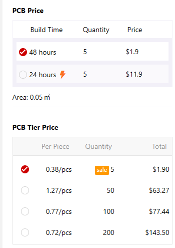
PCB mass production significantly affects the cost of custom PCB. The per-unit cost is typically higher for small-volume production, as manufacturers need to prepare specialized tools and setup for each run. Large-volume production can spread these fixed costs over more units, lowering the per-unit price. For example, the PCB cost per square inch is as low as $0.02, and the price decreases with higher quantities.
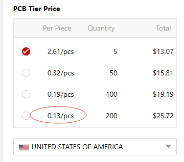
Impact of Production Volume on PCB Cost
PCB Cost impact: Mass production can reduce per-unit costs, making it an effective way to control expenses in large-scale production.
13. Lead Time
Fast turnaround times often place additional pressure on manufacturers, increasing costs. If the project requires urgent delivery, opting for expedited services may significantly raise overall expenses.
NextPCB provides 24-hour expedited service
14. IPC Level for PCB (IPC Class 2 and IPC Class 3)
The IPC Class level is a crucial factor in determining the price of custom PCBs. IPC (Institute for Printed Circuits) has established quality standard levels—Class 1, Class 2, and Class 3—that significantly affect the final product's cost. These classifications determine various aspects such as manufacturing processes, material selection, testing standards, and quality control requirements, all of which influence manufacturing costs, production cycles, and product reliability. IPC Class 2 PCBs, typically used for general commercial applications, have a simplified production process and relatively lower costs. In contrast, IPC Class 3 PCBs, designed for applications with extremely high reliability requirements—such as military, aerospace, and medical fields—demand more complex manufacturing processes, stricter material specifications, and more rigorous quality control, resulting in higher prices.
Main Differences between IPC Class 2 and Class 3:
| Aspect | IPC Class 2 | IPC Class 3 |
| Applicable Scope | The reliability standard for general electronic products, applicable to commercial and consumer electronics (such as home appliances, office equipment, etc.) | High-reliability applications (e.g., aerospace, military, medical devices) |
| Reliability Requirements | Medium reliability, suitable for general environmental use | Extremely high reliability, suitable for extreme environments and critical applications |
| Defect Tolerance | Allows some manufacturing defects as long as they don't affect functionality or long-term use | Virtually no tolerance for defects; any flaw could lead to failure |
| Manufacturing Process Control | Moderate process control, focusing on major issues and critical aspects | Strict process control, with attention to every detail and flawless execution |
| Design and Testing Requirements | Moderate design and testing requirements, typically meeting industry standards | Very high design and testing requirements, including extreme environmental and reliability tests |
| Environmental Adaptability | Suitable for standard environments, without considering extreme conditions like high temperatures | Requires design for extreme conditions, including high/low temperatures, humidity, electromagnetic interference, etc. |
| Quality Control | Moderate quality control, ensuring stable performance under normal conditions | High-level quality control to ensure the product's reliability and safety under any circumstances |
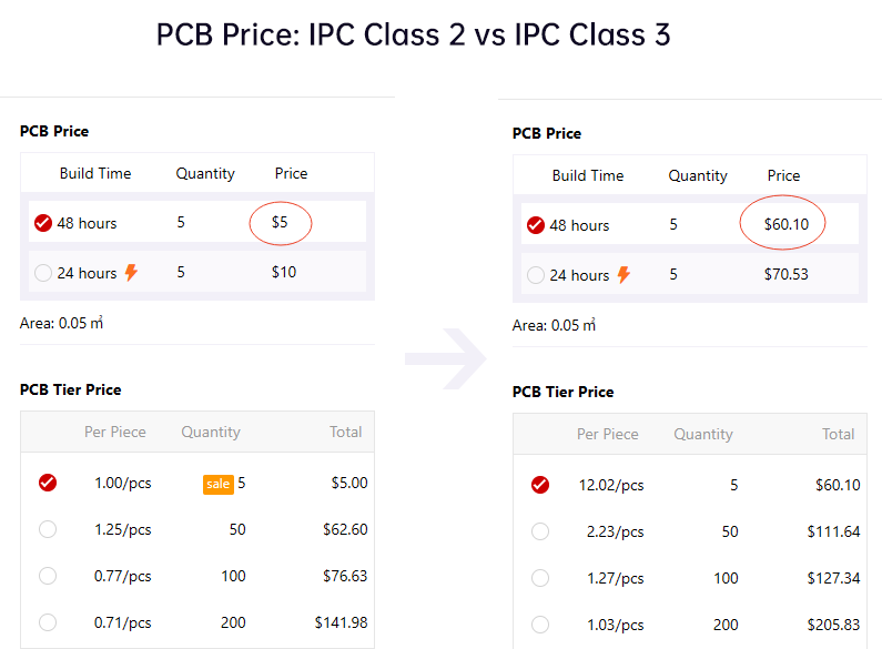
Impact of IPC Class Level on PCB Cost for 100x100mm, 5pcs
15. Other Custom Options Impacting PCB Costs
In addition to the commonly known factors influencing PCB manufacturing costs, several other aspects can affect production expenses. Below are some factors that may influence PCB costs:
a. Working Gerber Files
Working Gerber files are processed or modified Gerber files typically generated during the manufacturing preparation stage. These files have undergone CAM (Computer-Aided Manufacturing) adjustments, potentially including manufacturing compensation, process optimization, and other necessary modifications.
PCB Cost Impact: Since working Gerber files may require additional work from the manufacturer, there can be a slight increase in cost.
Gerber Files Knowledge Overview:Why gerber files are important for manufacturing
Manufacturers typically need the original Gerber files for adjustments and optimization. For example, if your original design has a line width of 6mil, but the file you send to the supplier shows a width of 6.6mil, this modified file is referred to as a "working Gerber" (used for production). Such files have been processed through CAM, potentially including manufacturing compensation, process optimization, and other necessary adjustments. Given that each manufacturer has its own engineering workflow, they may find these changes unclear.
- Original Gerber File: The file generated during the design phase, containing the designer's initial intent and all design details.
- Working Gerber File: This file has undergone processing and adjustment, including pre-production compensation and optimization.
- Why Factories Need Original Files: To ensure that all compensations and optimizations are correctly applied, manufacturers usually require the original design Gerber file. This helps prevent confusion or problems that may arise due to unclear modifications in the working files.
Check Your Gerber Files Online
b. Fabrication and Assembly Reports
Fabrication and assembly reports provide detailed information about the PCB’s manufacturing and assembly, including layer count, material specifications, via sizes, and more.
PCB Cost Impact: The level of detail in fabrication and assembly reports directly affects production accuracy and efficiency. Comprehensive reports can reduce misunderstandings and errors, ensuring a smooth production process and thus lowering costs. A lack of detailed reports may lead to production issues and increased costs.
c. X-out PCB
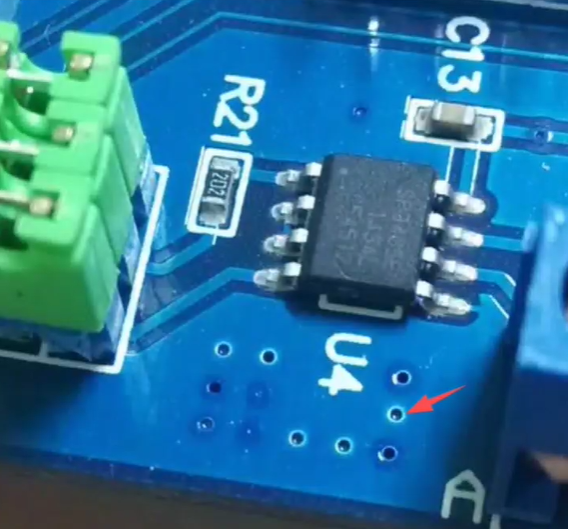
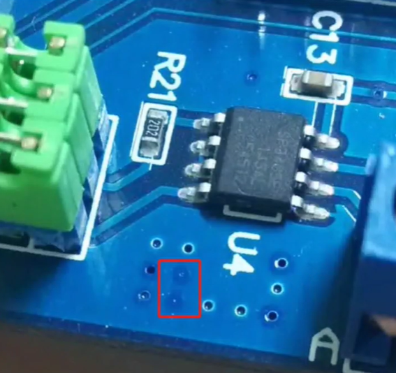
The "X" on a PCB indicates a "crossed board" (or X-out PCB), which refers to a defective board within a panel. This typically happens due to damage or misalignment during processing, cutting, or other production steps. The "X" marks the board as defective, often due to issues like short circuits, damaged pads, or broken traces.
Why not scrap the entire panel if only one board is defective? Scrapping the whole panel would increase costs. For example, if a panel contains 10 boards and one is defective, discarding the entire panel would be inefficient. Crossed boards are a common issue in panelization, as defects can arise at any stage of production.
As shown in the image, NextPCB's online PCB quote system provides corresponding options, and whether or not crossed boards are accepted will have an impact on the PCB price. Learn more about: Should I Accept Crossed Boards?
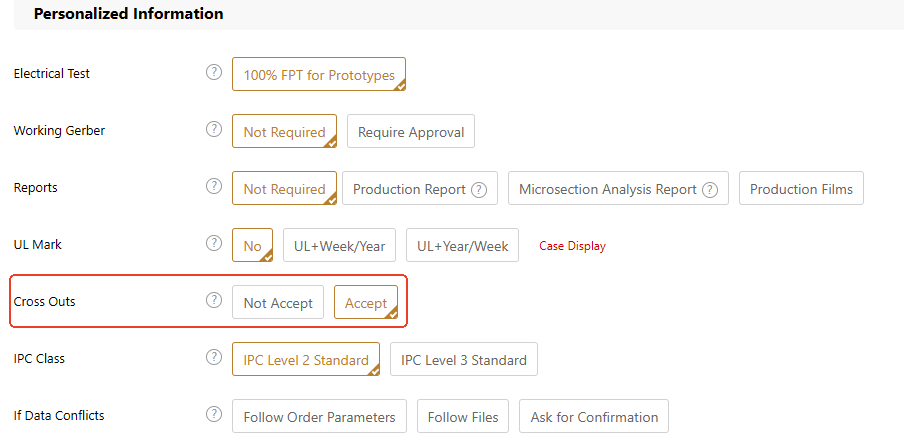
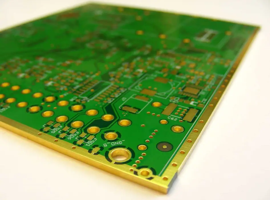
d. UL Mark (UL Certification)
The UL mark indicates that the PCB complies with UL’s safety standards. Additionally, UL certification facilitates product traceability, making it easier to identify the source of production and resolve any issues that arise.
PCB Cost Impact: Obtaining UL certification typically involves additional testing and validation, which can increase production costs. Fortunately, NextPCB offers a free UL certification option, which can be selected during the online PCB pricing process without adding extra costs.
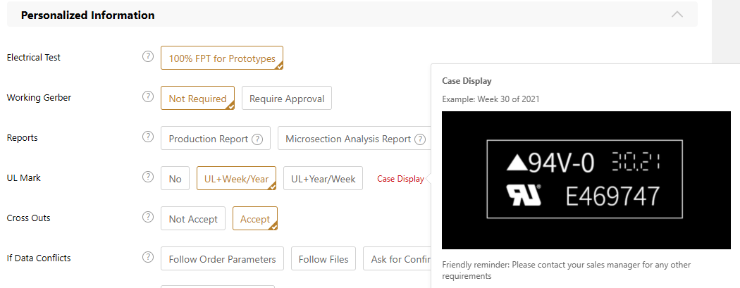
UL Marking Examples Provided by NextPCB
Check The Custom PCB Cost Online
What Factors Affect the Cost of Custom PCBA
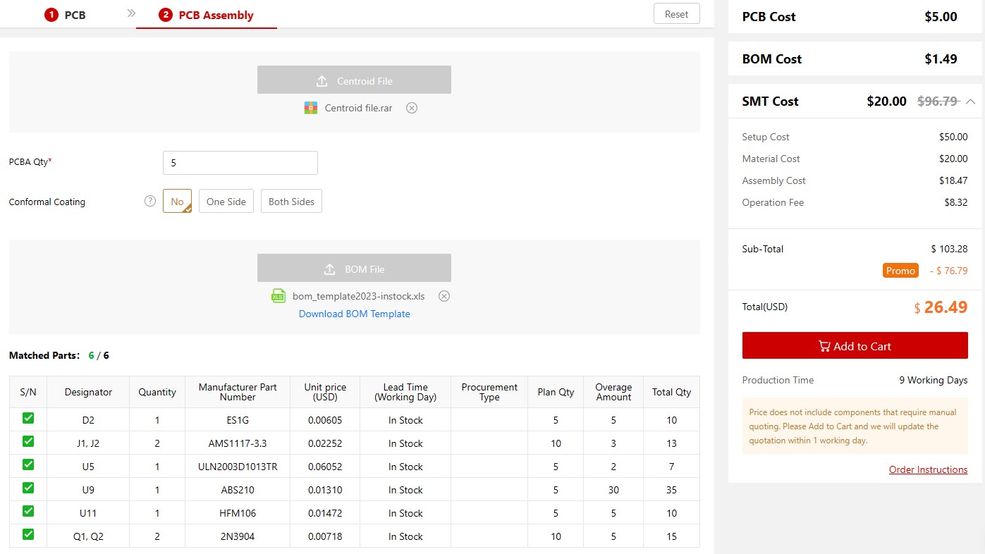
The cost of PCBA includes not only the manufacturing of the bare PCB board but also the procurement of components, assembly, soldering techniques, and testing. Below are the key factors affecting PCBA costs:
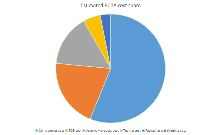
PCBA Cost Estimate Breakdown (For Reference Only)
a. Component Procurement Costs
The type, brand, and supply chain of components can impact procurement costs. High-performance components may be priced higher. The variety and quantity of components can also influence the cost.
PCBA Cost Impact: Selecting reasonably priced components or finding compatible alternatives can effectively control costs.
b. Assembly Process
PCB assembly process includes Surface Mount Technology (SMT) and Through-Hole Technology (THT). SMT is suitable for high-density and complex circuit designs, while THT is ideal for connections requiring higher strength.
- SMT: Suitable for high-volume automated production, offering faster speeds and relatively lower costs.
- THT: Requires manual soldering, typically used for low-volume, high-reliability applications, and incurs higher costs.
PCBA Cost Impact: Choosing the appropriate assembly process can optimize production efficiency and reduce assembly costs.
For a more detailed understanding of the PCB assembly, you can refer to the article "PCB Assembly - A Comprehensive Guide".
c. Testing and Quality Control
Testing during the PCBA process ensures the functionality and reliability of the product. Common testing methods include:
- Functional Testing: Verifies whether the circuit board functions as designed.
- In-Circuit Testing: Inspects solder joints and connections for proper assembly.
PCBA Cost Impact: Though testing adds to production costs, it significantly reduces the risk of future repairs and rework, ultimately saving money.
In addition to essential production processes such as E-test, AOI (Automated Optical Inspection), X-ray inspection, and manual inspection, NextPCB also offers free DFM (Design for Manufacturing) and DFA (Design for Assembly) services. Additionally, they provide free functional testing for up to 10 pieces.
How to Reduce Custom PCB and PCBA Costs
Design Optimization
Design optimization is key to reducing PCB and PCBA costs. By performing Design for Manufacturability (DFM) and Design for Assembly (DFA) checks, you can ensure the design is production-friendly and reduce issues during manufacturing.
- Reduce over-design: Avoid unnecessary complexity, such as excessive layers, small spacings, or redundant vias.
- Consider manufacturability: Choose materials and processes that are easier to manufacture.
- Standardize components: Use widely available, standardized components where possible to avoid the higher costs of custom components.
Volume Purchasing and Production
Increasing production volume is an effective way to lower per-unit costs. When long-term demand can be anticipated, ordering in bulk can help negotiate lower unit prices with the manufacturer.
For enterprise-level customers, NextPCB offers an pre-order service for components. This allows users to procure components at reasonable prices before starting mass production, reducing lead times and securing better pricing. Additionally, HQonline provides access to over 600,000 in-stock components, offering low prices and reliable quality.
Choose Reliable & Suitable PCB Manufacturers
Choosing the right PCB manufacturer plays an important role in cost control. Partnering with a PCB manufacturer with a well-established supply chain and technological capabilities ensures efficient production and reduces risks related to supply chain delays and additional costs. An experienced PCB Assembly manufacturer, equipped with a skilled engineering team, can offer comprehensive DFA review services to help identify potential optimization opportunities in your design, effectively reducing PCBA costs and improving production efficiency. NextPCB not only provides high-quality PCBA manufacturing services but also offers professional engineering support for your projects, ensuring that your design delivers superior performance while controlling costs for the best value.
Conclusion
Custom PCB and PCBA costs are influenced by a variety of factors, from material selection, layer count, and design complexity to component procurement, assembly processes, and testing. To optimize customization costs, businesses should consider these factors early in the design phase, selecting appropriate materials and processes and working closely with suppliers. Through thoughtful design optimization and bulk purchasing strategies, businesses can reduce costs without compromising on quality, ensuring timely, high-quality product delivery.