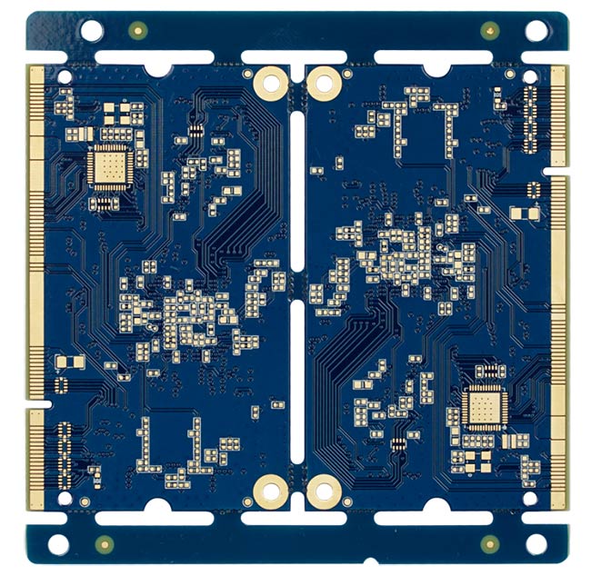
Features:
1) Years of experience in half-hole production, using Da Chuan Routing machine, routing the half-hole then routing the shape, meet the strict shape requirements;
2) Minimum line width and line spacing: 0.065/0.065mm, minimum BGA pad: 0.2mm, meet customer's special needs;
3) Electroplated Copper Filling of Blind Holes by Universal DVCP(Double Track Vertical Continuous Copper Plating Equipment ) to ensure that there are no voids in the holes and quality of customer products;
4) Strict sampling inspection mode, guarantee customers' product yield.
 PCB Assembly
 Layer Buildup
 Online Tools
 PCB Design-Aid & Layout
 Mechanics
 SMD-Stencils
 Quality
 Drills & Throughplating
 Factory & Certificate
 PCB Assembly Factory Show
Certificate


