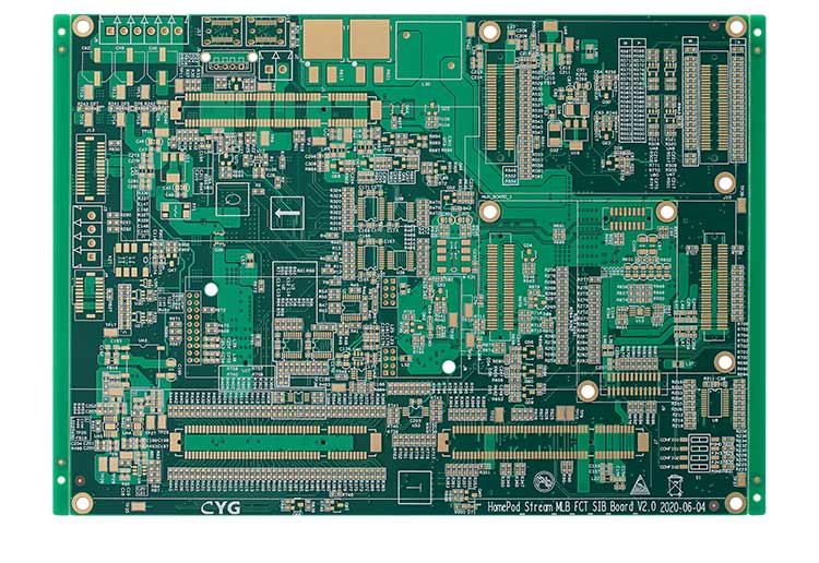
PCB is the abbreviation of the printed circuit board, which is the basic platform for carrying electronic components to realize corresponding functions. According to the substrate material, the PCB is manufactured according to the PCB design document, and the connection between the board layer, the board, and the component. The main function of the PCB is to play a full role in the electrical connections between all the components around the circuit board. Therefore, PCB is usually regarded as the core of electronic products.
The PCB should be manufactured in strict accordance with the PCB design files including Gerber files, NC drilling files, mold design files, etc., all of which will eventually form a real PCB. This article will provide a quick guide to PCB layout for PCB design beginners, covering key issues related to PCB design and layout.
What is the PCB layout
PCB layout mainly includes the placement of components on the board, routing, trace width, trace spacing, etc. Since PCB boards are used in almost all electronic products, therefore, PCBs have been widely used in consumer electronics, information, telecommunications, health care, even aerospace, and other fields. PCB layout plays a vital role in affecting its expected functions and performance.
The Basics of PCB layout
In the process of drawing schematic diagrams using PCB design software, it is essential to master the abbreviations of electronic devices, because the first three letters are usually used to represent a term. For example, RES stands for resistor; CAP stands for capacitor; IND stands for the inductor. Therefore, some electronic terms must be mastered: voltage, current, ohm, volt, ampere, watt, circuit, a circuit element, resistance, resistor, inductance, inductor, capacitor, capacitor, Ohm's law, Kirchhoff's law, Kiel Hough voltage law (KVL), Kirchhoff’s current law (KCL), loop, network, passive two-terminal network, active two-terminal network.
Inevitable problems in PCB layout
The PCB design should have a frame, and the minimum distance between the frame line and the component pins should be at least 2mm. It is also reasonable to set it to 5mm.
• Component placement
Basically, when it comes to a circuit system containing digital circuits and analog circuits, they should be separated so that the system is systematically coupled to circuits belonging to the same category. In addition, components should be placed according to signal flow, functions, and modules.
The input signal processing unit and output signal drive components should be placed on the side close to the board to keep the input/output signal lines as short as possible and reduce input/output interference.
As far as the component placement direction is concerned, components can only be placed vertically or horizontally. If there is a relatively high potential difference between the components, the distance between the components should be large enough to stop the discharge.
For medium-density circuit boards, the distance between low-power components should be considered based on soldering. When selecting wave soldering, the distance between components can be between 50mil and 100mil.
Power line and ground line design in the PCB layout
For PCB design engineers, it is not difficult to understand the cause of noise between the ground line and the power line. Even if the PCB layout is excellent, interference caused by insufficient consideration of power and ground wiring will still reduce product performance and even lead to complete failure. Therefore, the job of the PCB layout engineer is to reduce noise interference as much as possible, so as to ensure the quality of the product through the following methods:
- 1. A large area of the copper layer is used as a grounding wire, all unused ports should be grounded, and then used as a grounding wire. For multilayer PCBs, the power and ground wires should be arranged in different layers.
- 2. A decoupling capacitor should be added between the power line and the ground line.
- 3. The width of the ground wire and power wire should be set as much as possible. It is better to make the ground wire wider than the power wire. The width of the ground wire, power wire, and signal wire should be arranged as follows: ground wire>power wire>signal wire.
- 4. A wide ground wire should be used to form a loop on the PCB with digital circuits.
 PCB Assembly
 Layer Buildup
 Online Tools
 PCB Design-Aid & Layout
 Mechanics
 SMD-Stencils
 Quality
 Drills & Throughplating
 Factory & Certificate
 PCB Assembly Factory Show
Certificate


