
 PCB Assembly
 Layer Buildup
 Online Tools
 PCB Design-Aid & Layout
 Mechanics
 SMD-Stencils
 Quality
 Drills & Throughplating
 Factory & Certificate
 PCB Assembly Factory Show
Certificate
PCB Assembly Factory Show
Certificate
Support Team
Feedback:
support@nextpcb.comCopper pour in PCB design is a crucial step. It refers to filling the unused areas of a PCB with solid copper. The purpose of copper pour is to reduce ground impedance and enhance anti-interference capabilities, minimize voltage drop, improve power efficiency, and reduce loop area when connected to the ground.
The main advantage of copper pour is the reduction of ground impedance (a significant part of anti-interference is achieved by lowering ground impedance). In digital circuits, which have a lot of spike currents, lowering ground impedance becomes even more important.
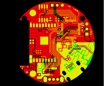
It is generally accepted that circuits composed entirely of digital components should have large areas of ground pour, while for analog circuits, copper pour can create ground loops, leading to electromagnetic coupling interference (except in high-frequency circuits). Therefore, not all circuits require copper pour.
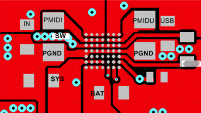
- EMC Requirements: Large areas of copper for ground or power planes can provide shielding effects. For specific ground types like PGND (Protective Ground), it serves a protective function.
- PCB Manufacturing: For manufacturing, copper pour is used to ensure even copper plating or prevent warping and deformation, especially for PCB layers with less routing.
- Signal Integrity: Copper pour provides a complete return path for high-frequency digital signals and reduces the routing for DC networks. Additionally, it aids in heat dissipation and can be required for mounting specific components.
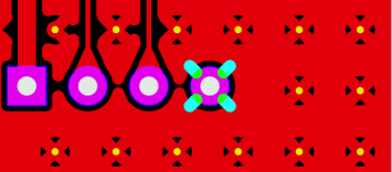
- Overheating during Rework: If the pins of components are fully covered with copper, heat dissipation may occur too quickly, making desoldering and rework difficult. To avoid this, a cross-shaped connection (with the pad and pin forming a "cross") is sometimes used.
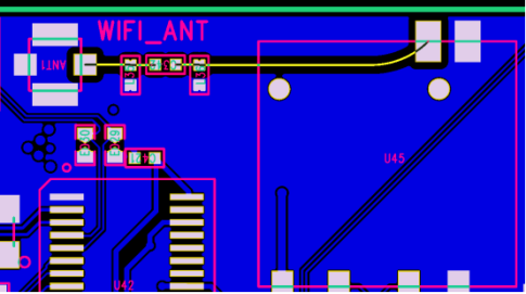
- Antenna Interference: Copper pour near antenna regions may weaken the signal or cause interference in signal acquisition. The impedance of copper pour can also affect the performance of amplifying circuits. Therefore, antenna areas typically do not have copper pour.
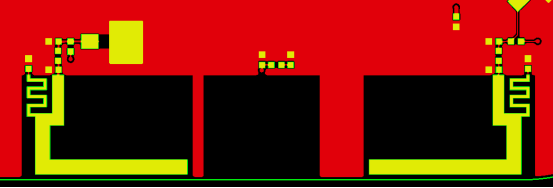
- Solid Copper Pour: This increases both current capacity and provides shielding. However, solid copper can cause stress from thermal expansion and contraction during wave soldering, leading to warping or bubbling. Slots are often added to relieve the tension.
- Grid Copper Pour: This mainly serves a shielding purpose but has less current-carrying capacity. From a heat dissipation perspective, grid copper reduces the heat absorption surface of the copper while still providing some electromagnetic shielding. However, the grid pattern must be carefully designed to maintain manufacturing quality, as overly small grids can reduce yield.
During PCB design, copper pour is generally used on every layer to prevent PCB warping and minimize signal interference and crosstalk. However, routing and components on the outer layers can divide the copper into smaller sections or narrow strips.
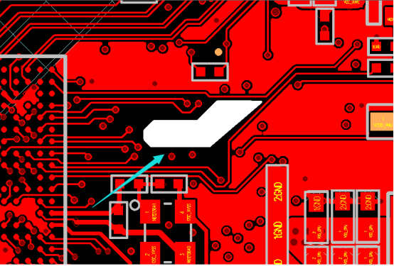
Thin, long, poorly grounded copper traces can act as antennas, causing EMC issues. Therefore, fragmented copper should be avoided during copper pour. If small fragments are created, they should be deleted.
Isolated copper (dead copper) is essentially equivalent to fragmented copper. If small, it should be removed. If large, it can be connected to the ground using vias to eliminate the issue of isolated copper.
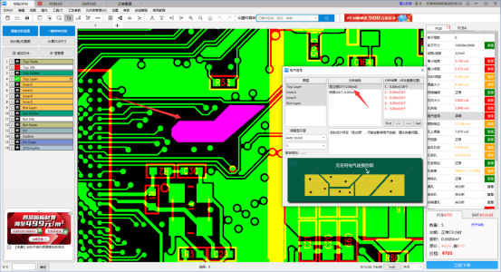
In PADS software, copper pour needs to be regenerated every time the design file is opened. This is because PADS stores copper pour data in a linear format, which can slow down the software. Only the outline of the copper pour is saved when the software is closed, and upon reopening, the copper pour must be regenerated.
- Hatch: Used to restore copper fill, as PADS only saves the copper outline, and the fill needs to be regenerated upon reopening.
- Flood: Used after the first completion of PCB layout or when the design rules are changed, requiring copper to be refilled.
- Plane Link: This is for internal layer copper pours, where the outline is saved, and the copper fill needs to be regenerated upon reopening.
When exporting Gerber files, copper pour must be regenerated to avoid missing copper pours in the Gerber, which could result in manufacturing errors and unusable products.
Fragmented or isolated copper can cause manufacturability issues. Thin copper traces may be etched away during production, leading to copper separation or short circuits. Isolated copper can cause additional communication between the design engineer and the PCB fabricator, increasing costs and delaying production.
Using DFM (Design for Manufacturing) software helps identify isolated copper in the design files before production, preventing errors, shortening production cycles, and reducing communication costs.
1. Loop Area Reduction: Copper pour reduces the overall loop area when connected to ground.
2. Ground Resistance Reduction: Copper pour reduces ground resistance and voltage drop, improving both digital and analog circuit performance. For high-frequency circuits, digital and analog grounds should be separated and connected using a single point with wire loops to minimize interference.
6. Considerations for Copper Pour
- For multiple grounds (SGND, AGND, GND), copper pour should be done separately based on the main ground type.
- Connections between different grounds should use 0-ohm resistors, ferrite beads, or inductors.
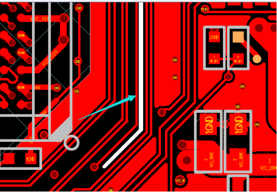
- Copper pour around the crystal oscillator, as it is a high-frequency source, should be grounded to the enclosure.
- Avoid sharp angles in copper traces as they can act as antennas from an electromagnetic field perspective.
- Metal components in the system, like heatsinks, must be well grounded.
- Three-terminal regulators and metal shields around oscillators should also be properly grounded.
In summary, if done correctly, copper pour offers more benefits than drawbacks by reducing signal interference and improving overall PCB performance.
Still, need help? Contact Us: support@nextpcb.com
Need a PCB or PCBA quote? Quote now
|
Dimensions: (mm) |
|
|
Quantity: (pcs) |
|
|
Layers: 2 |
Thickness: 1.6 mm |
|
|
|

 Printed Circuit Boards
 Surface

