Support Team
Feedback:
support@nextpcb.comFor any product design to achieve ultimate success, multiple inspections and tests are necessary at all stages of production. As said, the quality of PCBs is fundamental to the quality, functionality, and lifetime of electronic products. Therefore, testing is crucial in the PCB production process.
PCB testing primarily aims to address problems throughout the entire manufacturing and production process through a combination of manual and automated inspection methods. These types of tests can also be applied to prototypes or small-scale assemblies, helping identify potential issues in the final product.
Through testing, potential defects that may affect functionality, such as open circuits or shorts are not easily detectable by visual inspection. By greatly reducing significant issues, and identifying minor errors, you will save time, reduce defects and maximize the lifetime of your products.
Various testing methods for PCB boards:
1. Automated Optical Inspection (AOI)
Automatic optical inspection equipment, or AOI, is widely used in various industries and plays a critical role in PCB testing.
During the PCB production process, AOI is performed after etching the copper foil on the PCB board to form circuit patterns. The equipment scans the patterns on the board and compares them with the design files. It identifies the condition of the PCB board's surface patterns and compares them with the stored data in the AOI system. Any discrepancies are reported as defects, which are then confirmed and addressed by inspectors and manually repaired if necessary.
2. Flying Probe Testing
Flying probe testing is a recognized and effective form of in-circuit testing (ICT) that can efficiently detect production quality issues. It is a cost-effective testing method for improving circuit board standards.
Flying probe testing utilizes two or more independent probes that operate without fixed test points. These probes are mechanically controlled and move according to specific software instructions. Consequently, the initial cost of flying probe testing is lower compared to fixture testing. However, its testing efficiency is relatively lower since the probes move and test the points individually. Therefore, it is practical for small-batch orders.
3. Fixture Testing (Bed of nails):
A fixture is a specialized clamp designed based on the PCB board design for performing electrical continuity tests. It can be categorized as a single-sided fixture or a double-sided fixture.
In fixture in-circuit testing, metal probes within the fixture connect to the solder pads or test points on the PCB board. By applying power to the PCB board, typical values such as voltage and current of the test circuit are obtained to observe if the tested circuit is functioning properly. Fixture testing offers the advantage of high testing efficiency but comes with higher costs. Each PCB design requires a different testing fixture. Therefore, fixture testing is practical for large batch orders.
4. Visual Inspection:
Visual inspection is the most traditional method of inspection, primarily used for simple circuit boards. Its advantages include low initial costs and the absence of testing fixtures. It involves visually inspecting and determining the quality of PCB boards using magnifying glasses or calibrated microscopes. It helps identify whether the PCB board is acceptable and determines if repairs are necessary.
Visual inspection testing is limited to simple circuit boards and has disadvantages such as subjective human errors, high long-term costs, discontinuous defect detection, and difficulties in data collection. As PCB production increases and the spacing between wires and the size of components on PCBs decreases, visual inspection testing becomes less feasible.
Now, let us talk more about PCB Test Fixture Design.
Testing fixtures must be designed with positioning holes. The holes inside the board must be larger than 1.5mm to serve as testing positioning holes. Without positioning holes, the board may deviate during testing, leading to inaccurate results.
Positioning holes serve as the processing reference for PCB fabrication. Various methods are used to position PCB holes, mainly based on different positional accuracy requirements. Special graphic symbols should be used to represent positioning holes on PCBs. When requirements are not stringent, larger assembly holes on the PCB can be used as substitutes.
To facilitate drilling and milling the PCB and provide convenience for testing, many PCB manufacturers recommend design engineers include four non-metallic holes on the PCB. Positioning holes are usually designed as non-metallic holes with a drill diameter of 1.5mm or 2.0mm. If space is limited on the board, at least three positioning holes should be placed on three corners of the board.
For panelized boards, the entire panel can be treated as a single PCB, requiring only three positioning holes. Positioning holes can be placed on the breakaway rails of the panelized boards. If design engineers fail to include positioning holes, the PCB manufacturer may add them in areas that do not affect the circuitry or utilize existing non-metallic holes on the board as positioning holes.
Using HQDFM to make the most of testing procedures
DFM (Design for Manufacturability) guidelines provide specific recommendations for PCB design to ensure manufacturability from design to product. These guidelines include considerations such as component placement, trace routing, and the use of proper pad sizes and shapes. By following these guidelines, design engineers can minimize potential issues that may arise during testing, such as soldering defects or electrical shorts.
HQDFM is a free desktop suite developed by HQ Electronics to automate DFM checks and provide actionable feedback to designers before manufacture. HQDFM can assist with ensuring designs can be tested effectively.
Case Study:
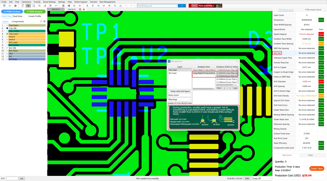
In-circuit testing relies on testing probes to make electrical contact with the pads on the circuit board. But the precision of the machines has its limits, combined with the thickness of the needle tip and the surface of the pad, pads that are too small cannot be reliably tested.

In this case, there are long pads with a width of 0.22mm. For pads less than 0.25mm in width, HQDFM recommends the user choose ENIG surface finish to help with testing and assembly as the surface finish is more planar compared to HASL.
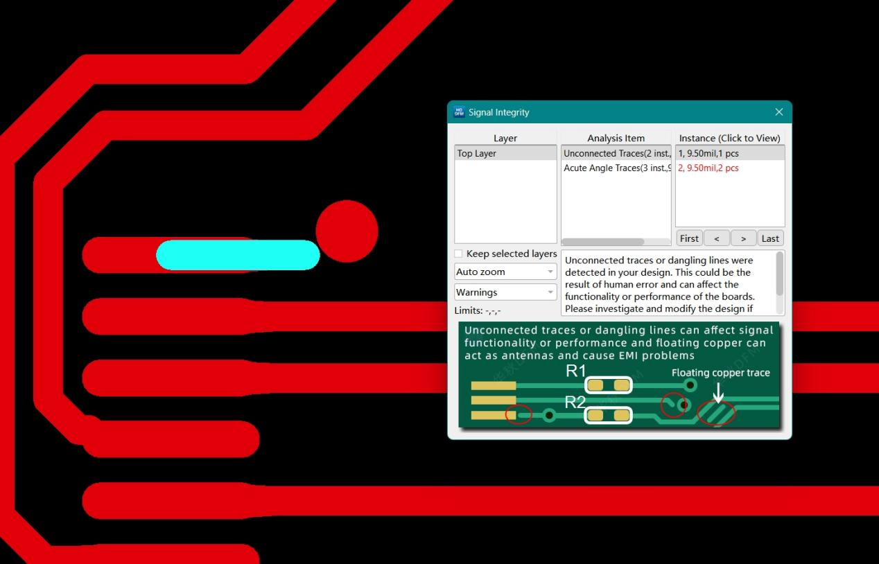
DFM can also help detect shorts and opens in the design. In-circuit testing compares electrical continuity with the design files, so if a short is present in the design, it will not be detected as an error during ICT. With that in mind, you can be sure that is all boards exhibit the same error, it is most likely a design mistake and not a manufacturing error.

By incorporating DFM principles and tools like HQDFM, and working closely with manufactures, design engineers can ensure the quality of their products and improve the overall quality and reliability of the final product.
Still, need help? Contact Us: support@nextpcb.com
Need a PCB or PCBA quote? Quote now
|
Dimensions: (mm) |
|
|
Quantity: (pcs) |
|
|
Layers: 2 |
Thickness: 1.6 mm |
|
|
|