

 Printed Circuit Boards
 Surface
 PCB Assembly
 Layer Buildup
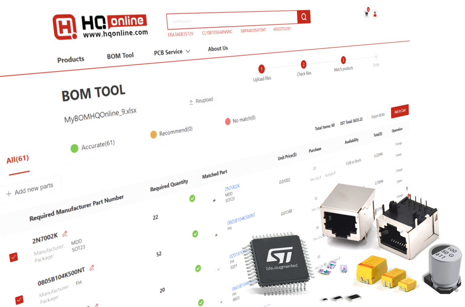
 Online Tools
 PCB Design-Aid & Layout
 Mechanics
 SMD-Stencils
 Quality
 Drills & Throughplating
 Factory & Certificate


-

-

-
-
-
-
-
-

-

-
-

-

-
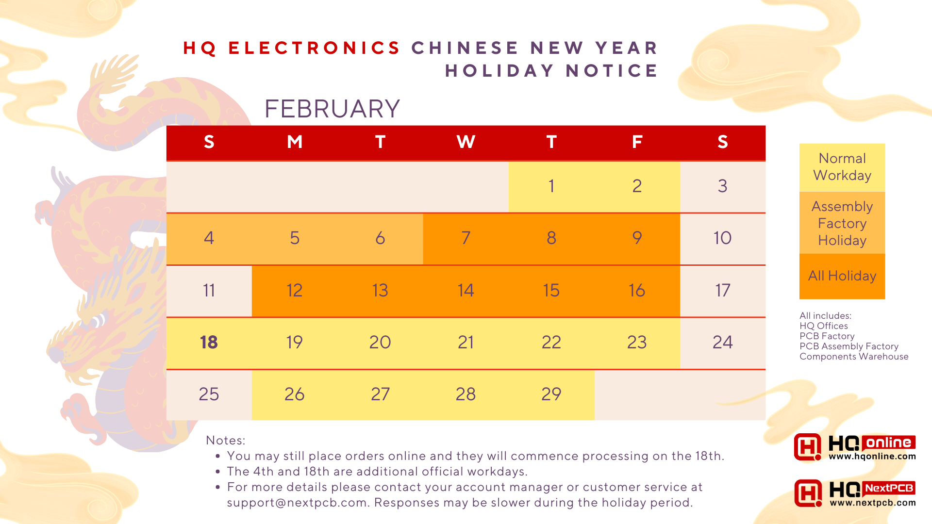
2023 Public Holidays Notice
NEXTPCB holiday on October 2023
1664 3 0 Shares
-
-
-
-

-
-
-

Categories
Recommended Article:
- RAK3172: The Ultimate LoRaWAN Module for IoT Applications in 2025
- Build Low-Cost FPGA Projects with Tang Nano 20K and Free PCBA Prototypes - NextPCB Accelerator #6
- NextPCB DFM Tool Exclusive Offer: Get a $10 Coupon Every Month!
- Unlocking FPGA Innovation with Tang Nano 20K: Features, Advantages, and Applications
- Developing world-class LoRaWAN solutions? Get preferential pricing & free prototypes on RAK3172 - NextPCB Accelerator #5
- Enhancing IoT Connectivity with SIM7600 Series
- Streamline Your PCB Design Workflow with KiCad Plugins from NextPCB
- Explore Embedded AI with ESP32-S3 and Free PCBA Prototypes - NextPCB Accelerator #4
- NextPCB Invigorates Partnership with KiCad Through Strategic Support and Innovation
- BC547 Transistor: Ultimate Guide for Engineers and Hobbyists
