What is High-frequency PCB
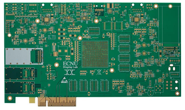
High-frequency PCB is a specialized circuit board used for the transmission of high-frequency signals, typically above 500MHz or 1GHz. It possesses excellent electrical characteristics and can provide stable and reliable signal transmission within the high-frequency range. It finds wide applications in wireless communication, radar systems, microwave communication, radio frequency identification (RFID), satellite communication, medical devices, and other fields. High-frequency PCBs have specific requirements in terms of material selection, design, and manufacturing processes to ensure the integrity and stability of signals during transmission.
Common Classifications of High-Frequency PCBs
High-frequency PCBs can be classified based on materials, applications, or design complexity. Common classifications include:
● Based on Materials: High-frequency PCBs typically use low-loss, low-dielectric constant materials to maintain signal quality. Examples include the use of PTFE (Polytetrafluoroethylene) or FR-4 high-frequency laminates.
● Based on Application Fields: This includes industries such as telecommunications, military and aerospace, and medical devices.
● Based on Design Complexity: Single-layer high-frequency PCBs, double-layer, or multi-layer high-frequency PCBs.
Structure of High-Frequency PCBs
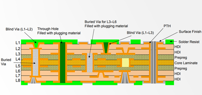
High-frequency PCBs have complex structures, typically including signal layers, ground layers, power layers, and insulation material layers. Multi-layer designs not only increase the wiring density of the board but also help in signal protection and minimizing interference. The material selection and layout design for each layer are crucial to ensure accurate transmission of high-frequency signals.
Why Choose High-Frequency PCBs and Its Pros and Cons
High-frequency PCBs play a crucial role in fields such as wireless communication, RF applications, radar systems, microwave communication, and medical devices. By providing a stable environment for high-frequency signal transmission, high-frequency PCBs meet the requirements of these applications for signal transmission quality, stability, and reliability, which cannot be achieved by traditional PCB boards. However, like any other PCB, high-frequency PCBs have their own advantages and disadvantages.
Advantages:
●Signal Integrity: High-frequency PCBs effectively manage the transmission of high-speed signals, reducing delays and signal losses.
●Strong Anti-Interference Performance: Through proper design, such as using specialized ground layouts, external interference can be significantly reduced.
●Flexibility and Compatibility: High-frequency PCBs can adapt to the demands of various high-speed, high-frequency applications and are compatible with a wide range of connectors and components.
Disadvantages:
●Design Challenges: High-frequency PCBs pose technical challenges to designers, requiring precise consideration of factors such as electromagnetic field effects and signal paths.
●Higher Cost: Compared to regular PCBs, high-frequency PCBs have higher material and production process requirements, resulting in increased costs.
Challenges and Solutions in High-Frequency PCBs Design
High-frequency PCBs design poses certain challenges, but these challenges can be overcome with various solutions. Here are some common challenges and their corresponding solutions. By following these principles and optimization methods, we can improve design quality and address common issues:
● The unity and stability of power and ground.
● Thoughtful routing and appropriate termination can eliminate reflections.
● Careful consideration of routing and suitable termination can reduce capacitive and inductive crosstalk.
● Noise suppression is required to meet EMC (Electromagnetic Compatibility) requirements.
In mitigating power noise, the following approaches can be taken:
● Pay attention to vias on the board: Vias require etching openings in the power layers to allow space for the vias to pass through. However, if the openings in the power layer are too large, it will inevitably affect the signal loops, forcing signals to detour, which increases the loop area and noise. Additionally, if several signal traces are concentrated near the openings, sharing this segment of the loop, common impedance will cause crosstalk.
● Ensure there are enough ground wires for the connections: Each signal should have its own dedicated signal loop, and the loop area between the signal and its return path should be as small as possible, meaning the signal and its return should run in parallel.
● Separate analog and digital power supplies: High-frequency devices are generally very sensitive to digital noise, so the two should be kept separate, joined only at the power entry. If a signal needs to cross between the analog and digital sections, a bypass loop can be placed at the crossing point to minimize loop area.
● Avoid overlapping separated power supplies across different layers: Otherwise, circuit noise can easily be coupled through parasitic capacitance.
● Isolate sensitive components: such as PLLs (Phase-Locked Loops).
● Place power traces: To reduce the signal loop area, placing power traces next to signal lines can help reduce noise.
By following these principles and optimization techniques, the design of high-frequency PCBs can be effectively improved, enhancing signal transmission quality and suppressing noise. In addition to these principles and methods, there are other optimization measures that can be taken:
● The fewer interlayer transitions between leads of high-frequency circuit components, the better.
"Fewer interlayer transitions" means minimizing the use of vias in the connection process of components. Reducing the number of vias can significantly improve speed and decrease the likelihood of data errors.
● The shorter the leads between high-frequency circuit component pins, the better.
The intensity of signal radiation is directly proportional to the length of the signal trace. The longer the high-frequency signal leads, the more susceptible they are to coupling with nearby components.
● The fewer bends in the leads between high-frequency circuit component pins, the better.
For high-frequency circuit routing, it is best to use straight lines for leads. If turns are necessary, 45-degree bends or arcs should be used.
● Be cautious of "crosstalk" introduced by signal lines running in parallel at close proximity.
High-frequency circuit routing should be mindful of "crosstalk," which refers to the coupling phenomenon between signal lines that are not directly connected but run in parallel closely to each other.
● Isolate high-frequency digital signal ground lines from analog signal ground lines.
When connecting analog ground lines and digital ground lines to the common ground, use high-frequency ferrite beads for connection or isolate them completely, choosing an appropriate location for a single-point interconnection.
● Add high-frequency decoupling capacitors to the power pins of integrated circuits.
Adding high-frequency decoupling capacitors to the power pins can effectively suppress high-frequency harmonic interference originating from the power pins.
● Avoid forming loops with routing.
All high-frequency signal routing should avoid forming loops; if unavoidable, the loop area should be minimized as much as possible.
● Ensure good signal impedance matching.
During signal transmission, impedance mismatches can cause signal reflections within the transmission channel. These reflections can lead to overshoot in the composite signal, causing fluctuations near the logic threshold.
The Future Trends of High-Frequency PCB
The future trends of high-frequency PCB are influenced by various technological and market-driven factors. For example, there is a strong correlation between current high-frequency PCB technology and the AI industry, which together drive the development and innovation of AI hardware. As AI technology continues to evolve and market demand grows, high-frequency PCB will continue to play a crucial role in supporting various high-performance and efficient AI applications and solutions.
Here are potential future development trends in high-frequency PCB design:
● Higher operating frequencies: With the increasing demand in communication technology, RF applications, and high-performance computing, high-frequency PCBs need to support higher operating frequencies.
● Lower transmission loss: As the demand for data rates and bandwidth increases, high-frequency PCB designs will need to reduce signal transmission loss. This can be achieved through the use of low-loss materials and optimized layout designs.
●Advancements in integration technology: Integration of high-frequency PCBs with packaging will be a future trend to improve signal transmission efficiency and reduce signal loss, enabling more compact and efficient high-frequency system designs.
● Material innovation: To meet the requirements of higher frequencies and lower loss, future high-frequency PCBs may adopt new materials that have lower dielectric constants and higher thermal conductivity, suitable for high-power and high-frequency applications.
● Environmental friendliness and sustainability: With the growing awareness of environmental protection, high-frequency PCB designs will pay more attention to the environmental friendliness and sustainability of material selection, production processes, and waste disposal.
● Security and reliability: For critical applications such as aerospace, medical, and defense, the security and reliability of high-frequency PCB designs will be of paramount importance, and the corresponding requirements will continue to increase.
 PCB Assembly
 Layer Buildup
 Online Tools
 PCB Design-Aid & Layout
 Mechanics
 SMD-Stencils
 Quality
 Drills & Throughplating
 Factory & Certificate
 PCB Assembly Factory Show
Certificate


