
 PCB Assembly
 Layer Buildup
 Online Tools
 PCB Design-Aid & Layout
 Mechanics
 SMD-Stencils
 Quality
 Drills & Throughplating
 Factory & Certificate
 PCB Assembly Factory Show
Certificate
PCB Assembly Factory Show
Certificate
Support Team
Feedback:
support@nextpcb.com
When we refer to "full board gold plating," we typically mean "electroplated gold," "electroplated nickel-gold board," "electrolytic gold," "electro-gold," or "electro-nickel-gold board," with distinctions between soft gold and hard gold (hard gold is generally used for gold fingers).
The process involves dissolving nickel and gold (commonly called gold salt) in a chemical solution, immersing the PCB in an electroplating bath, and applying current to generate a nickel-gold coating on the copper surface of the PCB. Electroplated nickel-gold is widely used in electronic products due to its high hardness, wear resistance, and resistance to oxidation.
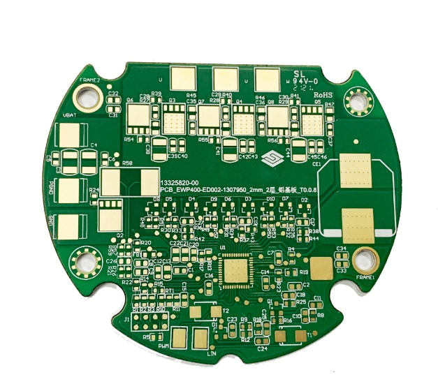
Gold plated pcb
What is the PCB Immersion Gold ?
Immersion gold generates a coating through a chemical redox reaction, typically resulting in a thicker gold layer. It is a type of chemical nickel-gold deposition process that can achieve a relatively thick gold layer.
Immersion Gold: The immersion gold process uses chemical deposition, where a coating is formed on the PCB surface through a redox reaction. This process generally involves several stages, including pre-treatment, nickel deposition, gold deposition, and post-treatment. In the overall PCB production process, the immersion gold process occurs after the solder mask step, as the gold deposition is applied only to the PCB pads, not the entire board surface.
Gold Plating: Gold plating is based on electrolysis, also called electroplating. It involves immersing the PCB in a chemical solution containing nickel and gold and applying an electric current to deposit a nickel-gold layer on the copper surface. The gold plating process happens before the solder mask step, as it targets the entire copper surface of the PCB.
Immersion gold pcb
Immersion Gold: The crystal structure formed by immersion gold is denser, and the gold layer is typically thicker, ranging from 0.025-0.1 µm. This results in a more vibrant and aesthetically pleasing appearance.
Gold Plating: The gold plating layer is thinner, and its crystal structure may differ from immersion gold. The appearance of gold-plated boards may seem slightly whiter, lacking the rich golden hue of immersion gold.
Immersion Gold: PCBs with immersion gold exhibit excellent solderability. The gold layer is easy to solder, minimizes soldering defects, and allows better stress control, reducing potential issues caused by uneven stress distribution.
Gold Plating: The solderability of gold-plated PCBs is generally inferior, and poor soldering performance is one of the main reasons many companies opt out of gold plating.
Immersion Gold: Due to the stable properties of gold and the dense crystal structure, immersion gold PCBs are less prone to oxidation, enhancing the PCB’s durability and reliability.
Gold Plating: While gold plating offers some level of oxidation resistance, it may not be as stable as immersion gold.
Immersion Gold: The immersion gold process only targets the pads and does not impact signal transmission. The signal's skin effect ensures transmission occurs mainly within the copper layer, making immersion gold PCBs perform well in terms of electrical characteristics.
Gold Plating: Gold-plated PCBs also show good electrical performance, but potential soldering issues may limit their application in certain areas.
6. Wear Resistance
Immersion Gold: The gold layer in immersion gold is relatively softer, so immersion gold PCBs may be less wear-resistant compared to gold-plated PCBs. For parts that require frequent plugging and unplugging, such as gold fingers, immersion gold boards might wear out more quickly.
Gold Plating: The gold plating layer is usually harder, providing better wear resistance, making it more suitable for environments with high mechanical stress.
7. Cost and Applications
Immersion Gold: The immersion gold process is more expensive but offers superior solderability, oxidation resistance, and electrical performance. It is widely used in high-performance circuit boards such as keypads and gold-finger boards.
Gold Plating: The gold plating process is less costly, though limited by its poorer solderability in some applications. It is still used in cost-sensitive products like remote control boards and toy boards.
Which is the better choice ?
Gold Plating Process: Its advantages include lower cost, good wear resistance, suitability for high-temperature environments, and strong repairability, making it ideal for mass production. Gold plating offers good conductivity, enhancing signal transmission, and provides a visually appealing appearance, making it suitable for high-end products. However, direct contact between metals can lead to diffusion, increasing the risk of short circuits, and it may not be ideal for high-frequency applications.
Immersion Gold Process: Known for its high reliability, excellent conductivity, strong compatibility, and high flatness, the immersion gold process is suitable for various substrate materials, including FR4, high TG, and ceramics. The dense crystal structure of the gold layer resists oxidation and does not cause short circuits. However, the cost is higher, and it may not be suitable for high-temperature environments due to the risk of metal diffusion and short circuits.
In summary, for applications requiring high performance and reliability, immersion gold is likely the better choice as it provides superior electrical connections, signal transmission, and solderability. For cost-sensitive, high-volume production environments, gold plating may be more appropriate due to its lower cost and good wear resistance. The key is to choose the most suitable process based on specific application needs and budget constraints.
Still, need help? Contact Us: support@nextpcb.com
Need a PCB or PCBA quote? Quote now
|
Dimensions: (mm) |
|
|
Quantity: (pcs) |
|
|
Layers: 2 |
Thickness: 1.6 mm |
|
|
|

 Printed Circuit Boards
 Surface

