
 PCB Assembly
 Layer Buildup
 Online Tools
 PCB Design-Aid & Layout
 Mechanics
 SMD-Stencils
 Quality
 Drills & Throughplating
 Factory & Certificate
 PCB Assembly Factory Show
Certificate
PCB Assembly Factory Show
Certificate
Support Team
Feedback:
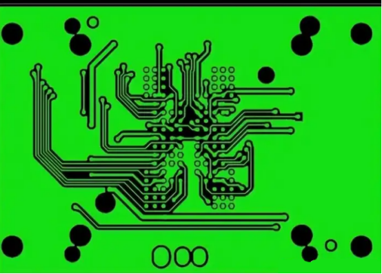
support@nextpcb.comPCB warpage refers to the deformation of a printed circuit board (PCB) from its intended flat shape. PCBs are typically made from fiberglass and composite materials, and most are only laminated once, resulting in simple structures. Warpage can be visually identified when the PCB deviates from its designed geometry.
According to the IPS standards, the allowable warpage (WD) for PCBs intended for mounting should be less than or equal to 0.75%. If the WD exceeds this value, the board is deemed warped or defective. For situations where no components are installed and only through-hole components are used, the warpage standard can be relaxed to less than or equal to 1.5%. Some manufacturers, aiming to meet higher customer demands, may enforce stricter standards, with some requiring a WD of less than or equal to 0.5%, or even 0.3%.
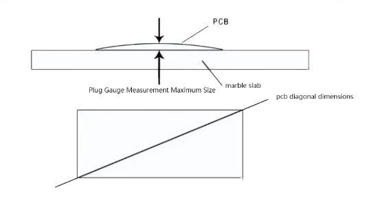
3. Calculating PCB Warpage
Warpage indicates whether the PCB is flat enough to fit perfectly into mounting holes and surface mount pads. It typically refers to the deformation of the board's surface from its designed shape. Various factors influence warpage, so careful attention during production is essential to avoid scrapping the entire board due to minor errors.
Warpage Calculation Formula:
Warp = Single Corner Warp Height / (PCB Diagonal Length * 2) * 100%
4、Causes of PCB Warpage
Warpage during PCB manufacturing can arise from both thermal and mechanical stresses:
Tin furnace temperature 225℃-265℃, common board hot air solder leveling time 3s-6s. hot air temperature is 280℃-300℃.
After the solder leveling, the board is put into the tin furnace from room temperature, and after it comes out of the tin furnace, it will be washed in room temperature after treatment within two minutes. The whole hot air solder leveling process is a sudden heating and cooling process.
Due to the different materials and uneven structure of the boards, thermal stresses inevitably occur during cooling and heating, resulting in microscopic strains and overall deformation warping areas.
PCB boards in the semi-finished stage of storage, are generally firmly inserted in the shelves, the tightness of the shelves are not adjusted, or the storage process of the board stacking will lead to mechanical deformation of the board.
Especially the thin plate below 2.0mm, the impact is more serious.
When the board length of 80 mm or more without copper, the board thickness is less than 1.0 mm, will lead to board warping.
If the board can not be pressed together, and can not be thickened, the use of heavy warpage.
When the board has too many hollow locations and the board is too large, it is easy to bend after reflow.
In the manufacturing process of PCBs, there is an even distribution between all dielectric layers. However, it is the uneven distribution of the copper layers that causes PCB warpage to occur. To prevent warpage
The design engineer must balance the copper pattern on each layer of the board with the area of the circuit. The design engineer must also balance component layout, assembly distribution, and thermal distribution to minimize warpage.
For example, if the outermost top surface has a large copper surface and the outermost bottom surface has very few copper traces, the PCB will have a greater tendency to warp after etching. The design engineer must ensure that the wire pattern areas of the two outer layers match as closely as possible. If there is a large difference in copper area between the two sides, it is best for the designer to add a separate copper grid on the thin side to balance the two.
Suggestions: copper plating in the hollowed out areas to reduce board warpage; in addition, if the inside of the board does not affect the function, copper should also be laid down; the last suggestion is to add process edges and lay down copper on the side of the process.
The core board and PP board of multi-layer board must be of the same brand, otherwise the board will warp.
For example, the 6-layer board pp sheet asymmetry: 2-3 core board pp sheet thin, 4-5 core board pp sheet thick, so that a pressure on the warping was pressed out. Therefore, the core board and PP sheet must be of the same brand to ensure the thickness is consistent and the symmetry of the PP sheet of the multi-layer board.
The manufacturer must ensure that the alignment of the prepregs between the layers remains symmetrical. For example, for a six-layer sheet, it is desirable to have the same thickness between layers 1-2 and 5-6, including the number of prepreg sheets. This will prevent warpage after lamination.
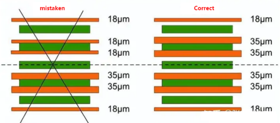
The arrangement of the layers of prepreg remains symmetrical
The purpose of baking the PCB (150°C for 8±2 hours) before cutting the copper-clad laminate is to remove the moisture from the board, and at the same time make the resin in the board fully cured, further eliminating the residual stress in the board, which is useful for preventing the board from warping.
Currently, many double-sided and multilayer boards still insist on the baking step before or after discharging. However, there are exceptions in some board factories. Currently the drying time in PCB factories is also inconsistent, ranging from 4-10 hours. It is recommended that the decision be made based on the grade of the printed circuit board being produced and the customer's requirements for warpage.
Bake the whole piece and then cut into puzzles or undercut and then bake, both methods are feasible. It is recommended to bake the board after cutting and the inner board should also be baked.
After prepreg lamination, the shrinkage rate is different in the warp and weft directions, and the warp and weft directions must be differentiated when dropping and laminating, otherwise it will easily cause the finished boards to warp after lamination, and it will be difficult to correct it even if pressure is applied to the baked boards.
Many of the causes of warpage of multi-layer boards are due to the fact that there is no distinction between warp and weft direction of the prepreg when laminating and it is stacked randomly.
How to distinguish between warp and weft? Rolled prepregs are rolled in the warp direction, and the width direction is in the weft direction; for copper-clad boards, the long side is in the weft direction, and the short side is in the warp direction. If you are not sure, check with the manufacturer or supplier.
After hot and cold pressing, the multilayer boards are removed, cut or milled to remove burrs, and then laid flat in an oven at 150°C for 4 hours to gradually release stresses within the board and to allow the resin to cure completely, a step that should not be omitted.
0.4 ~ 0.6mm ultra-thin multi-layer plate for surface plating and pattern plating, should make a special pinch roller. After clamping the thin plate on the pinch rollers in the automatic plating line, clamp the whole pinch rollers with a round bar. String the rollers together and straighten all the plates on the rollers so that the plates will not be deformed after plating.
Without this measure, after plating 2 0 to 30 um copper layer, the plates will bend and it is difficult to remedy.
PCBs that are leveled with hot air are subjected to high temperatures (about 250°C) from the solder bath. After removal, it should be placed on a flat marble or steel plate for natural cooling, and then sent to a post-processing machine for cleaning, which helps to prevent the board from warping.
In some factories, in order to improve the brightness of the lead-tin surface, the boards are put into cold water immediately after hot-air leveling, and then removed for post-processing after a few seconds. This hot and cold shock may cause some types of board warpage. warping, delamination or blistering.
In addition, an air-float bed can be installed on the device for cooling.
In the PCB process, boards with large warps are picked up by a roll leveler and flattened before moving on to the next process. Many PCB manufacturers have found this practice to be effective in reducing the warpage of the finished PCB.
For finished products, the warpage is obviously too bad to be leveled with a roll leveler. Some PCB factories will be put into a small press (or similar fixtures) in order to press the warped PCB board, stay a few hours to ten hours for cold press leveling, from the practical application, the effect of this practice is not very obvious. First, the leveling effect is not very large, and secondly, after flattening the board is easy to rebound (i.e., warpage recovery).
Some PCB factories will be a small press heated to a certain temperature, and then the flattening of the PCB board for hot pressing, the effect will be better than cold pressing, but the pressure is too large will lead to deformation of the wire; if the temperature is too high will produce rosin discoloration and its discoloration and other defects. Moreover, whether cold press leveling or hot press leveling, it takes a long time (a few hours to a dozen hours) to see the results, flattened PCB board warping rebound ratio is also very high.
The hot press flattening method with bow mold is recommended here. Depending on the area of the PCB to be flattened, a simple bow mold is used (see Figure 1). Here, two types of leveling operations are proposed.
The warped PCB board is bent to face the curved surface of the mold, and the fixture screws are adjusted so that the PCB board is deformed and warped in the opposite direction, and then the mold with the PCB board is put into the oven to be heated to a certain temperature for baking for a while. In the heating conditions, the substrate stress gradually relax, the deformation of the PCB board back to a flat state. However, the baking temperature should not be too high, so as to avoid rosin discoloration or substrate yellowing. However, the temperature should not be too low, at lower temperatures to completely relax the stress needs a longer time.
Generally, the glass transition temperature of the substrate can be used as the reference temperature for baking. The glass transition temperature is the phase transition point of the resin, at which the polymer chain segments can be rearranged to fully relax the substrate stress.
Because the leveling effect is so pronounced, the advantage of flattening with a bow mold is that the investment is minimal. Ovens are available in PCB factories. The leveling operation is very simple. If the number of warps is large, it is enough to make several bow molds. You can put them in the oven once. With fewer molds, the drying time is shorter (a few minutes or so), so the leveling operation is more efficient.
For PCB boards with relatively small warpage deformation, you can put the PCB boards to be leveled into an oven that has been heated to a certain temperature (i.e., the temperature setting can refer to the vitrification of the substrate).
Still, need help? Contact Us: support@nextpcb.com
Need a PCB or PCBA quote? Quote now
|
Dimensions: (mm) |
|
|
Quantity: (pcs) |
|
|
Layers: 2 |
Thickness: 1.6 mm |
|
|
|

 Printed Circuit Boards
 Surface

