
 PCB Assembly
 Layer Buildup
 Online Tools
 PCB Design-Aid & Layout
 Mechanics
 SMD-Stencils
 Quality
 Drills & Throughplating
 Factory & Certificate
 PCB Assembly Factory Show
Certificate
PCB Assembly Factory Show
Certificate
Support Team
Feedback:
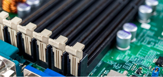
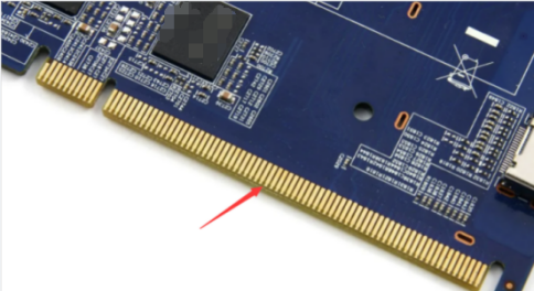
support@nextpcb.comOn computer memory sticks and graphics cards, there's a row of golden conductive contacts known as PCB“Gold Fingers.” In the PCB design and manufacturing industry, "Gold Finger" (or Edge Connector) refers to the part of a connector that serves as the outlet for external connections of a PCB.
How much do you know about pcb "Gold Finger"? Today, we'll walk you through the design of "Gold Finger" in PCBs, along with key details about its manufacturability.
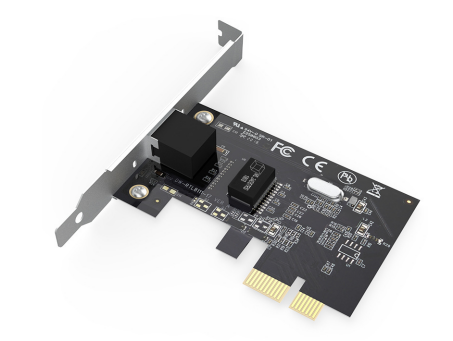
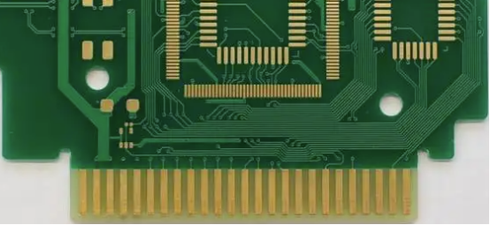
When auxiliary PCBs (such as graphics cards or memory sticks) are connected to the motherboard, they interact with slots like PCI, ISA, or AGP, transmitting signals between peripherals or internal cards and the computer.
"Gold Finger" enhances the functionality of the motherboard by allowing secondary PCBs like memory, graphics, sound, and network cards to connect via the slot, transmitting high-quality graphics and audio. Since these cards are rarely disconnected or reconnected, the PCB "Gold Finger" typically outlasts the card itself.
Peripheral devices such as speakers, subwoofers, scanners, printers, and monitors are connected to the motherboard via "Gold Finger." These devices use specific ports (HDMI, DisplayPort, VGA, DVI) which in turn are linked to the PCB on the motherboard.
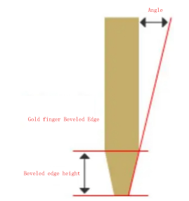
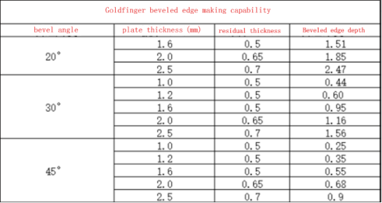
- The distance between the PCB "Gold Finger" and the board edge must be safe. This depends on the board thickness and the chamfer angle, which is typically 45 degrees.
- If the PCB "Gold Finger" is too close to the edge, copper must be cut according to certain parameters to avoid exposure. To prevent shortening the PCB "Gold Finger," design its distance from the board edge based on specified safe distances.
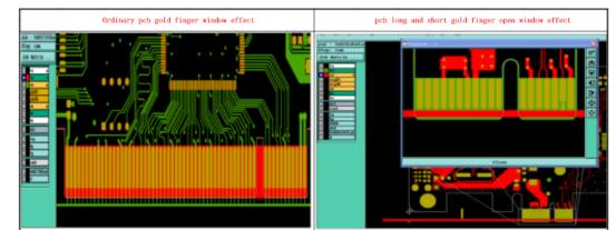
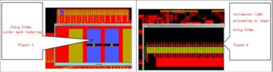
To facilitate card insertion, the PCB "Gold Finger" area is left without a solder mask, fully opened up. Without this, solder resist ink may accumulate between PCB "Gold Fingers" and peel off during repeated insertions, leading to poor contact with the slot.
- The window for "Gold Finger" and "Tin Finger" should be about 10 mil larger than the edge of the board.
- The solder mask opening should be 4 mil larger than the circuit trace on each side, ensuring it doesn’t expose copper.
- No solder mask openings are allowed within 2 mm of the PCB "Gold Finger."
To aid card insertion, the board outline near the "Gold Finger" should have a beveled or rounded edge. This prevents the sharp edges from damaging the slot during insertion, thus improving product reliability.
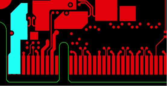
Avoid copper pours on the outer layer in the PCB "Gold Finger" area to ensure easy card insertion. If multiple "Gold Fingers" share the same network and are connected via copper, the result may be a single large block instead of individual "Gold Fingers," complicating insertion and removal.
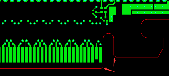
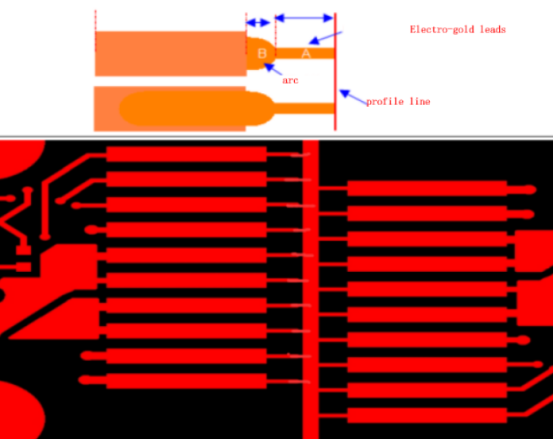
- The primary lead of a long PCB "Gold Finger" is 40 mil, and the secondary lead is 20 mil, with a connection point of 6 mil. The spacing between the "Gold Finger" pad and the 20 mil lead is 8 mil. After adding leads to the long and short PCB "Gold Fingers," the primary lead should be moved 8 mil away from the long "Gold Finger."
- When the primary lead enters the PCB, it should be connected using diagonal lines. If there is a large groove beside the "Gold Finger," the lead should be rounded, not right-angled.
- If the single board size of the PCB "Gold Finger" panel is smaller than 40x40mm, the board must be chamfered first, followed by milling the outline. The chamfering process requires positioning holes on both sides of the electroplated edge for precise milling during the second outline process.
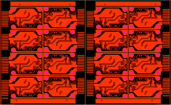
- When panelizing, use a notch design to expose the PCB "Gold Finger" outward. When panelizing for PNL, position the "Gold Finger" inward to facilitate adding gold plating traces.
The process includes: material cutting – inner layer imaging – inner layer etching – inner layer AOI – browning – lamination – drilling – copper deposition – panel plating – outer layer imaging – pattern plating – outer layer etching – outer layer AOI – solder mask printing – solder mask imaging – solder mask inspection – silkscreen – solder mask imaging 2 – immersion gold – "Gold Finger" plating – surface QC – stripping – outer layer imaging 2 – developing 2 – outer layer etching 2 – stripping – board milling – "Gold Finger" chamfering – electrical testing – final inspection – shipping.
- For multilayer PCBs involving "Gold Finger" (gold contacts), the copper stacking in the "Gold Finger" area of regular products should be 80 mil, while optical products and memory sticks should have 40 mil.
- For products without PCB "Gold Finger" processing but requiring chamfers, the copper stacking should follow "Gold Finger" requirements.
- The "Gold Finger" trace width is 12 mil and compensates with the circuit. For electrical "Gold Finger," the width is 40 mil, with the length the same as the trace.
- For optical products with the "Gold Finger" + gold plating process, the pad trace is not compensated, and the "Gold Finger" should be ≥0.5mm from the board edge. If the board thickness tolerance is ±0.1mm, additional auxiliary copper is required in the panel gap around the "Gold Finger," with a 0.4mm non-metallic hole added at the corner of the PCB "Gold Finger" outline.
The thickness can range from 3-50u", offering excellent conductivity, oxidation resistance, and wear resistance. It is commonly used in PCBs that undergo frequent plugging and unplugging or in areas subject to mechanical friction. However, due to high costs, it is limited to "Gold Finger" or localized gold plating.
Common thickness is 1u" but can reach up to 3u". Due to its superior conductivity, flatness, and solderability, it is widely used in high-precision PCBs with button positions, IC bonding, BGA designs, and "Gold Finger" PCBs with lower wear resistance requirements. The cost of immersion gold is lower than that of electroplated gold, and it has a characteristic golden-yellow color.
In addition to the manufacturability design considerations mentioned above, issues related to "Gold Finger" design can be detected before production using Huaqiang’s DFM (Design for Manufacturability) software. This helps mitigate potential manufacturability issues during production.
Since PCB "Gold Finger" products typically have high costs, manufacturing errors that go undetected until final product stages can result in significant losses. Thus, pre-production design file checks using HQDFM software are critical for reducing costs and improving production efficiency.
Still, need help? Contact Us: support@nextpcb.com
Need a PCB or PCBA quote? Quote now
|
Dimensions: (mm) |
|
|
Quantity: (pcs) |
|
|
Layers: 2 |
Thickness: 1.6 mm |
|
|
|

 Printed Circuit Boards
 Surface

