
 PCB Assembly
 Layer Buildup
 Online Tools
 PCB Design-Aid & Layout
 Mechanics
 SMD-Stencils
 Quality
 Drills & Throughplating
 Factory & Certificate
 PCB Assembly Factory Show
Certificate
PCB Assembly Factory Show
Certificate
Support Team
Feedback:
support@nextpcb.comFiducial marks, also known as reference points or optical alignment marks, are key features used by pick-and-place machines during PCB assembly. They help these machines and inspection equipment accurately identify the position and orientation of the PCB, ensuring that components are placed correctly. These optical marks are usually located at the edges or specific areas of the PCB.
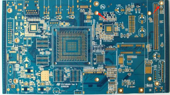
When preparing for PCB fabrication, we typically send the Gerber files to the manufacturer. If the PCB also needs to be assembled with components, we must provide a Bill of Materials (BOM) and a Pick-and-Place (PNP) file. Automatic pick-and-place machines use this data and need to identify one or more physical points on the PCB. Fiducial marks enable the machine to place components more accurately, reducing reliance on machine tolerances or human errors.
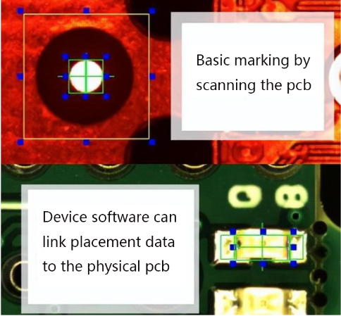
Fiducial marks on a PCB are reference standards used by automated machinery such as Surface Mount Technology (SMT) machines and Automated Optical Inspection (AOI) systems. These marks consist of a solitary copper pad isolated from other visible landmarks. Without fiducial marks, machines might either misplace components or refuse to operate altogether. By reading fiducial marks placed on the PCB, automated equipment can determine the exact placement or scanning position for components.
Technically, most machines do not actually "read" the components on the PCB; instead, they recognize the reflection from the fiducial mark's pad.
Global fiducial marks are used to position all circuit features on a single board and differentiate between the circuit patterns and the PCB reference. They are based on a three-network system, with the reference point positioned at the lower-left corner (0,0), and the other two marks along the X and Y axes.
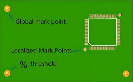
Local fiducial marks are primarily used for aligning components with many pins or with a fine pitch (less than 0.65mm between pin centers), providing auxiliary alignment.
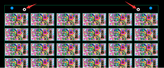
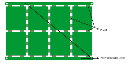
These are used in mass production during panelization to assist in aligning all circuit functions for multiple boards assembled on a single panel.
Fiducial marks are commonly circular for several reasons:
- Circular shapes are easier for machines to detect.
- In HAL (Hot Air Leveling) finishes, circular marks maintain their shape better than square ones, which can deform.
- Machines find it easier to locate the center of a circle.
- Circular marks have the smallest surface area.
- Circular shapes etch uniformly.
- Circular marks are less prone to rotation errors than irregular shapes.
- Circular mounting holes can also serve as inexpensive fiducial marks.
Machines using vision systems need to accurately locate the fiducial mark, and the circular shape is optimal for this purpose.
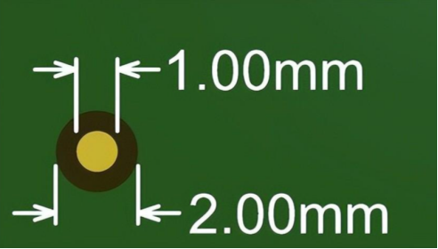
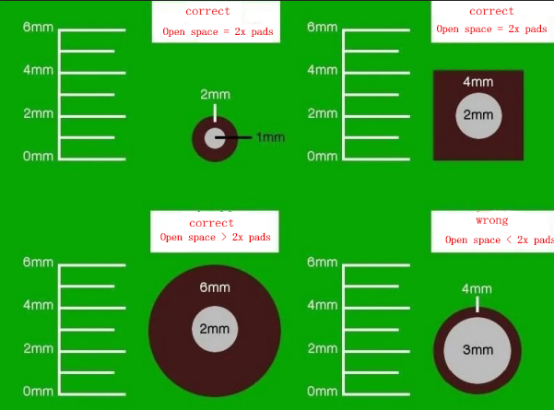
The size of fiducial marks can vary depending on the assembly machine being used. Typically, a solder mask opening diameter of 3.2mm with a bare copper diameter of 1.6mm, or a 2mm solder mask opening with a 1mm bare copper diameter, is sufficient for most machines.
The fiducial marks on the same PCB should not differ in size by more than 25 microns. The clearance area around the fiducial mark should be at least twice the radius of the mark.
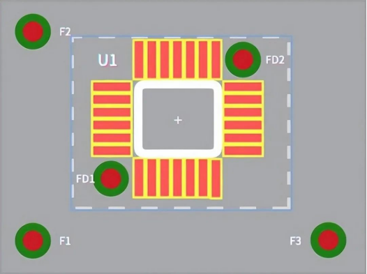
Manufacturers often recommend adding three fiducial marks at the corners of the PCB, as this provides two angle alignment measurements and helps the pick-and-place machine infer the correct orientation. Fiducial mark size should be consistent across both global and local fiducials on the same board, and the variation should not exceed ~25 microns.
For two-layer boards, the fiducial marks on the top and bottom layers should align perfectly. The sizes of the fiducial marks, including the solder mask opening, should be the same on both sides.
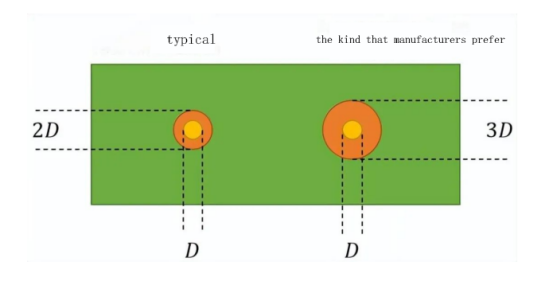
Local fiducial marks are often as small as 1mm in diameter, with a 2mm solder mask opening. The D-3D rule applies here, as some manufacturers prefer larger solder mask openings.
Local fiducials generally do not exceed 1mm in size, allowing for routing and space for other components. For small components like 0201 resistors or BGA chips, local fiducials may not be needed as the assembly machine can place them accurately without additional references.
Fiducial marks should not be placed too close to the edges of the PCB. Pick-and-place machines use clamps to hold the PCB in place during assembly, and if a fiducial mark is covered by the clamps, it can cause problems. It is recommended to place fiducial marks at least 3mm (preferably 5mm) from the PCB edges to avoid these issues.
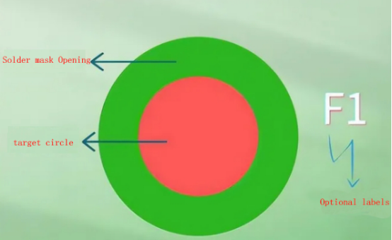
Fiducial marks consist of three main parts:
- A solid copper pad on the top or bottom copper layer.
- A circular opening in the solder mask, which serves as the alignment target.
- Optional side text labels for additional information.
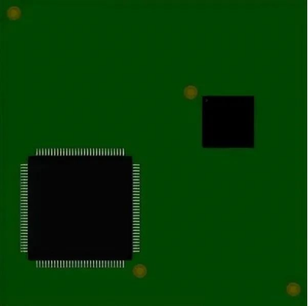
Fiducial marks should be placed at the four corners or diagonally across the PCB to form multi-point alignment, with maximum distance between marks for the best accuracy.
- PCB Fiducial Marks: The placement of fiducial marks is determined by the PCB transmission method in the pick-and-place machine. When using a conveyor to move the PCB, marks should not be placed near the clamping areas or positioning holes.
Area marker cannot be located
- Local Fiducial Marks: For components with over 100 pins (like QFP packages), two fiducial marks should be placed diagonally. For QFP components with more than 160 pins, four fiducial marks (one at each corner) are recommended.
Proper clearance around the fiducial mark is essential. An open area (free of copper, solder mask, silkscreen, etc.) around the pad helps the camera pick up the mark without visual interference. The open area should have a diameter at least twice the size of the pad.
Fiducial pads should be finished with the same metal used on the rest of the PCB. Remember, fiducial marks reflect light, so they should not be covered by solder mask, silkscreen, or any other material.
Using three fiducial marks is the optimal number to eliminate potential misalignment between the stencil and the PCB.
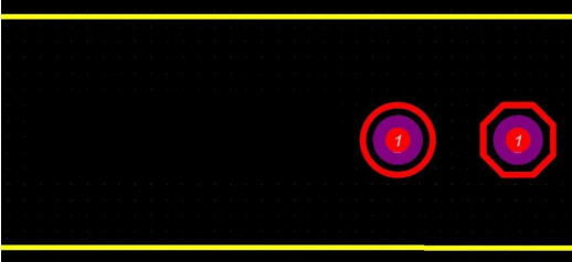
- One Fiducial Mark: With only one fiducial mark, the machine cannot determine the correct PCB rotation. A PCB with only one fiducial mark will not run properly.
- Two Fiducial Marks: While two fiducial marks allow the machine to operate, there are risks. The two-mark setup offers decent but not excellent positioning accuracy. Also, the PCB could be loaded in reverse, and the machine may still recognize the fiducials, potentially causing component misplacement or equipment damage.
- Three Fiducial Marks: This is the best setup. A third fiducial mark allows triangulation, improving overall accuracy and eliminating the risk of the board being loaded in the wrong orientation.
- Four Fiducial Marks: Although adding a fourth fiducial mark seems like it could improve accuracy, it rarely provides additional benefits and could reintroduce issues like detecting inverted panels.
Fiducial pads must have a smooth finish to reflect a uniform image. The copper marks should be plated with the same metal finish used on the rest of the board. While processes like plating and immersion are reliable in terms of uniformity, Hot Air Solder Leveling (HASL) tends to have greater variability.
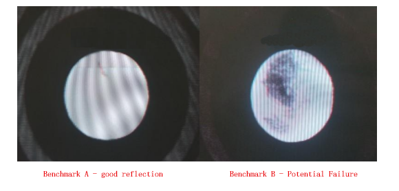
Any variation in the finish's thickness can affect reflection accuracy. Addressing this issue may require extra production time, potentially leading to software adjustments or reworking the fiducial marks altogether.
Optimal performance is achieved when there is high contrast between the fiducial marks and the PCB substrate material. The background surrounding all fiducial marks must remain consistent.
This guide provides a comprehensive overview of designing, understanding, and utilizing fiducial marks to improve the precision and efficiency of PCB assembly processes.
Still, need help? Contact Us: support@nextpcb.com
Need a PCB or PCBA quote? Quote now
|
Dimensions: (mm) |
|
|
Quantity: (pcs) |
|
|
Layers: 2 |
Thickness: 1.6 mm |
|
|
|

 Printed Circuit Boards
 Surface

