
Support Team
Feedback:
support@nextpcb.comThanks to the PCBs flexibility, it is fairly easy to bend or shape the board Solder Mask Material. This makes them ideal for cases where complex geometric shapes are required.
You'll learn everything you need to know about solder masks in this comprehensive article. You'll also find out how a solder mask can help with problems, such as relief during the soldering process. Lastly, you'll learn how to make your own solder mask and where you can get custom-colored masks, finished boards, and PCB assembly services for your project.
For any type of PCB, it's important to have a protective coating on top of the copper traces. This prevents oxidation and protects the copper, so it can continue to be resistant to environmental contaminants. Resin is a smart choice for your solder mask because it's durable, effective against humidity and insulation, maintains good looks over time, and can withstand high temperatures.
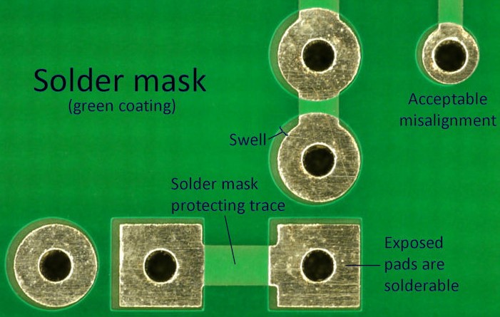
Some people use the color green to define solder mask material, but actually, it's a color of oil. Nevertheless, different colors are available for solder masks, such as green, blue, black, and white. The type of color you use depends on different usages.
For example, designers will typically use a red solder mask on prototypes in the New Product Introduction (NPI) stage. This lets the PCB stand out, making it easier to distinguish from mass-produced products. Black solder masks are often selected when PCBs should be partially or fully visible to meet their end product's color palette.
A solder mask or stencil, depending on your preference, acts as your PCB's primary protector against corrosion and oxidation. It improve the PCB quality by preventing performance degradation and shortening of electronic lifespan. More importantly, a solder mask creates a barrier between soldered joints and other conductive aspects of the PCB during assembly, thereby preventing the formation of solder bridges.
If a circuit is hand-made, you will not see solder masks, but they are always present in mass-assembled PCBs. The solder mask material resembles the copper layer and is added on when using machinery to these boards such as a bath. Solder masks are often considered separate layers of the PCB because they can be seen transparently in a finished board when one looks through any of the non-copper layers.
Solder mask is a protective coating applied over the PCB copper traces during manufacturing. Each layer of the paint contains a polymer material that ensures the quality and operation of your device's circuits. There is more than one type of solder mask, and which one you choose depends on your budget and what functionality you need. The most common solder-mask option is printed with an epoxy adhesive that protects all of the PCBs conductors.
This is a list of the most common types of solder masks:
If you carefully analyze other PCB solder mask guides, you will discover two more solder masks – the top-side and bottom-side masks. Generally, they refer to the solder masks applied on the upper and lower PCB sides, respectively. They do not refer to any fabrication method or material.
As we have mentioned earlier, a liquid epoxy solder mask Material is the most common option in printed films. Apart from being a popular solder mask option, this liquid epoxy film is also the cheapest method available. To create this type of solder mask, you use a woven mesh to support ink-blocking patterns and the liquid epoxy polymer hardens during thermal curing. The dye used in this solder mask will cure to its chosen color.
You can use the LPSM method when applying a dry film solder mask Material. In both cases, the solder masks are exposed to a photographic process. Instead of being used in liquid form, the dry film is applied in sheets of solder mask film using vacuum lamination. The process compels the unexposed solder mask film to stick to the PCB, eliminating bubbles from the film.
When the solder mask is lightly exposed, you need to remove the unexposed sections with a solvent and then cure the remaining film with heat.
The high-quality, photoresist-like solder mask material is either applied via a film or as a liquid. This process will create openings for pads and vias. Anytime you're creating holes that have smaller diameters than the hole you've punched in the board, using LPSM like epoxy or spraying it over the board is an inexpensive option. However, there's a more accurate technique of using lithography to define solder mask openings and fine details like pads and vias.
In the LPSM method, you have to create a mask from your Gerber files for your preferred solder mask. You should also carefully clean your panelization boards to remove any hardened dust on your solder mask. Aside from that, cover every panel as liquid LPSM cures.
To dry PCBs before exposing them to UV light, you'll first want to place them in an oven and let them sit on a rack at 265 degrees Fahrenheit. Next, place a photography mask over the dry PCB and then use UV light to expose it. The exposed LPSM will be cured by UV light while the covered parts are washed away with solvent which creates the blank layer.
Solder masks can be any color, with the most common colors being green and black. However, there are more colors available to satisfy design requirements like telling prototypes apart from final products or make an enclosure match your company's color theme. Additionally, many OEMs have begun introducing new equipment and processes in their factories. Reflecting these changes in the manufacturing process, solder masks also come in random colors to give your products a unique feel.
Only these five colors are common for a solder mask: white, black, red, yellow, and blue. Clear is often used nowadays instead of white or black. Aside from these five colors, NEXTPCB can also provide other custom choices if the customer wants to make those changes.
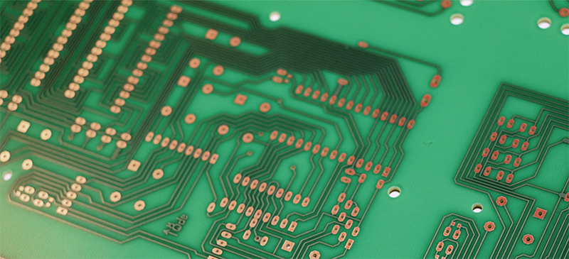
A solder mask color is used for the circuitry in a PCB. Though the array of colors has changed over the last five years, green is still the most popular. The primary reason for this is that inspection is easier with greener color. Research has shown that green stands out more to human eyes and facilitates an easier review of copper pads, traces and blank spaces.
Green masking tape is a solid choice when it comes to masking, compared to other types. It cures correctly, sticks well, and displays the highest resolution. This means that it can create minor damages in a wide board.
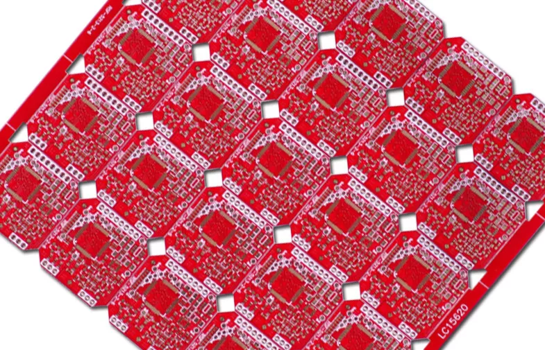
Red solder masks are the preferred choice for many designers, including those from the fields of Artificial Intelligence and the Internet of Things. This may be because red creates a stronger contrast than other colors. It could also be because red sparks creativity and is just aesthetically pleasing.
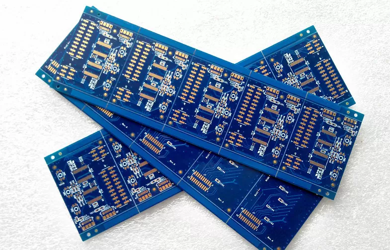
There are many similarities between blue and green solder masks. However, more designers choose to use the color blue because it's more uncommon on the market. Blue PCBs are rare, but NEXTPCB can make custom boards with this solder mask color.
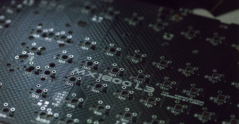
Though black solder masks don't catch your eye, they do last longer and protect circuitry that needs to maintain durability, like headlights. Since black paint absorbs heat more than other colors, the solder of a black PCB will be less likely to reflow during a soldering process.
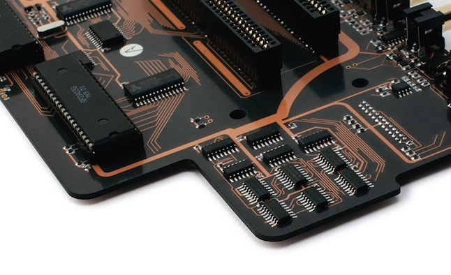
If you can't find the perfect color for your project, then we provide rarer yet more unique options. For example, our purple, yellow, and orange solder mask gives your product an appearance that is only seen in niche electronics industries.
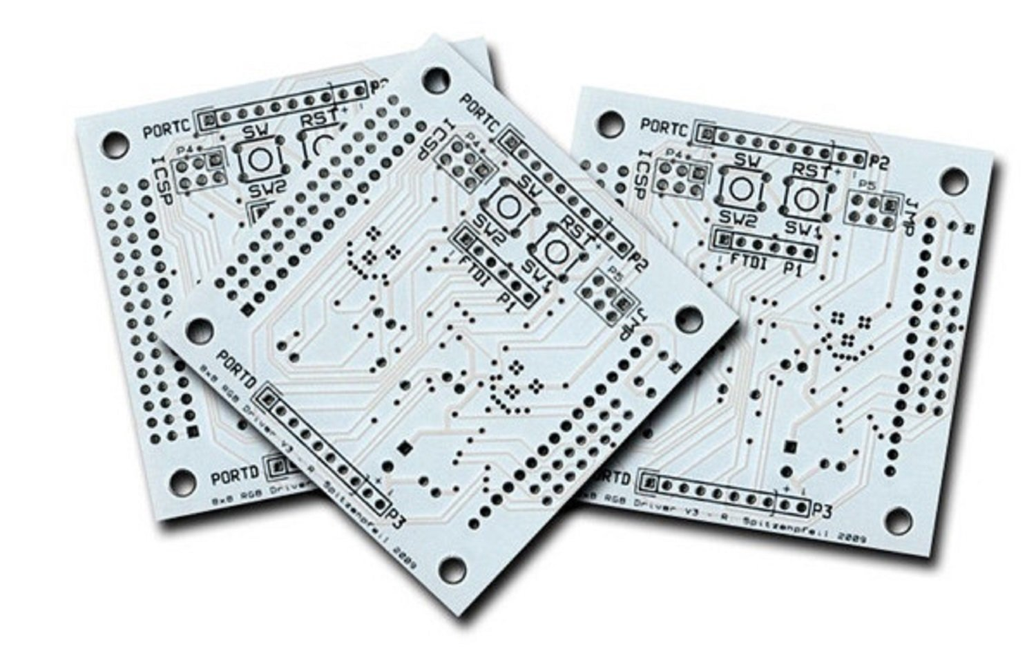
White solder masks are rarely applied because they offer poor visibility. Many low-quality masks will turn yellow after some time, especially when exposed to high temperatures for an extended period of time. That being said, white solder masks are usually ideal for LED systems because they are brighter than any other color.
In PCB design, the solder mask material must be created as a separate layer in your Gerber files. Since negative images are used for all the mask layers, any colored areas on your board will not be covered by a solder mask. This is not a problem because the solder mask layer will show you where not to apply it, based on the shapes and regions of your board.
Generally, you're going to want to cover the whole PCB with solder masks, excluding the regions for mounting components and maybe the points you plan to use as test points. The sensor pinhole aperture depends on your product, but you'll want to adjust the mask so that it's 4 mils wider than the copper pad. If you print your solder mask at the same size as these pads, it's going to be centered incorrectly and they might overlap some of those pads.
If you're looking for a PCB manufacturer with the experience needed to manufacture, fabricate, and assemble your PCBs, Nextpcb is the perfect choice. We have years of experience with solder mask color and design recommendations. All you have to do is request an online quote and we'll provide detailed suggestions for your PCB layout design.
Still, need help? Contact Us: support@nextpcb.com
Need a PCB or PCBA quote? Quote now
|
Dimensions: (mm) |
|
|
Quantity: (pcs) |
|
|
Layers: 2 |
Thickness: 1.6 mm |
|
|
|