
 PCB Assembly
 Layer Buildup
 Online Tools
 PCB Design-Aid & Layout
 Mechanics
 SMD-Stencils
 Quality
 Drills & Throughplating
 Factory & Certificate
 PCB Assembly Factory Show
Certificate
PCB Assembly Factory Show
Certificate
Support Team
Feedback:
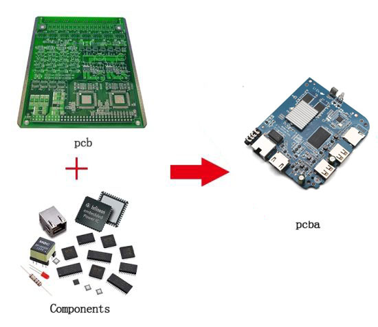
support@nextpcb.comPrinted Circuit Boards (PCB), also known as printed wiring boards, are essential electronic components. They act as the foundation for electronic devices, providing mechanical support and electrical connections for various electronic components. PCBs are named "printed" because they are made using electronic printing techniques. But what exactly is PCBA?
PCBA stands for the Assembly of PCB. It refers to the complete process of mounting components onto a bare PCB board through Surface Mount Technology (SMT) and then through-hole components via Dual In-line Package (DIP) processes. Typically, strict functional testing is required to ensure that the PCBA operates correctly.
In this article, we'll explore the entire journey from a bare PCB to a fully assembled PCBA.
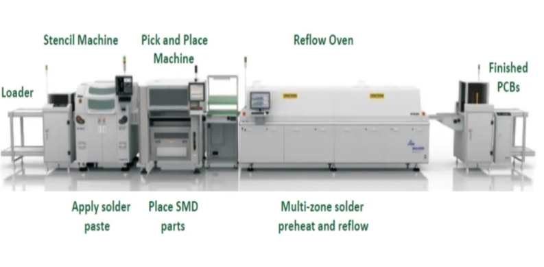
Surface Mounted Technology (SMT) is a method used in the electronics industry to mount components directly onto the surface of the PCB. This process involves placing surface-mount components (SMC/SMD) on the board and securing them using soldering techniques like reflow soldering or wave soldering.
Preparation Before SMT:
Once these preparations are complete, the SMT process can begin. The PCB is loaded into the machine, and the mark points are used to orient the board correctly. Solder paste is applied to the stencil, and the paste is deposited onto the PCB's pads. The pick-and-place machine then positions the components on the board according to the programmed instructions. Finally, the board undergoes reflow soldering to create a secure connection between the components and the board.
After this, an automatic optical inspection (AOI) is performed to check for defects like solder bridging, misaligned components, or improper polarity. However, functional tests are not conducted at this stage since the board may still require through-hole components.
Note: Some components have specific polarities or pin arrangements, so incoming material inspection is critical to prevent placement errors, especially for components like Ball Grid Array (BGA) packages, where mistakes can be time-consuming to correct.
Dual In-line Package (DIP) refers to through-hole components that are inserted into the PCB and soldered. These components typically have leads that go through holes in the board.
Preparation Before DIP:
The DIP process is simpler than SMT but requires manual labor to insert components into the board. After insertion, the board goes through wave soldering, where the components are securely attached to the PCB.
After the SMT and DIP processes, the PCBA undergoes functional testing to ensure it operates as intended.
Step 1: Visual Inspection - A preliminary inspection is done to identify visible issues such as solder bridges, cold solder joints, or missing components. Problematic boards are sent for rework, while functional boards proceed to the next step.
Step 2: Electrical Testing - Using test fixtures, the PCBA is subjected to functional tests. Power is applied to the board, and various tests are conducted, such as checking relay activation and communication signals. This step ensures that each module on the PCBA functions correctly.
By conducting these two steps, not only can defective boards be identified, but the exact issues can also be pinpointed, reducing the workload for subsequent repairs.
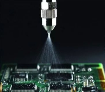
To protect the PCBA from environmental factors like moisture, dust, and corrosion, it undergoes a protective coating process. This could involve applying conformal coating (three-proof paint) or dipping in wax.
Different companies may use various methods, such as manual brushing, machine spraying, or dipping. In some cases, no protection is applied, depending on the application.
From a bare PCB to a fully functional PCBA, each step in the process involves careful preparation, execution, and testing to ensure the final product meets quality standards. By following these steps, manufacturers can ensure the reliability and performance of their products in various applications.
Still, need help? Contact Us: support@nextpcb.com
Need a PCB or PCBA quote? Quote now
|
Dimensions: (mm) |
|
|
Quantity: (pcs) |
|
|
Layers: 2 |
Thickness: 1.6 mm |
|
|
|

 Printed Circuit Boards
 Surface

