
 PCB Assembly
 Layer Buildup
 Online Tools
 PCB Design-Aid & Layout
 Mechanics
 SMD-Stencils
 Quality
 Drills & Throughplating
 Factory & Certificate
 PCB Assembly Factory Show
Certificate
PCB Assembly Factory Show
Certificate
Support Team
Feedback:
support@nextpcb.com1. What is PCB Hot Air Solder Leveling (HASL)?
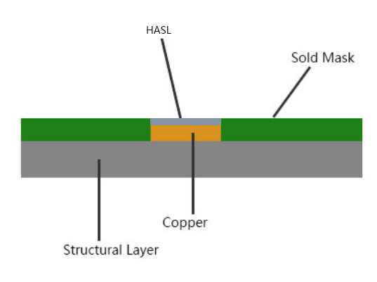
Hot Air Solder Leveling (HASL) is a surface finish process for PCBs. It involves applying a layer of tin-lead alloy to the copper surface of the PCB, which helps protect the pads from oxidation and maintains solderability. The solder used in HASL typically consists of 63% tin and 37% lead, which melts and bonds with solder paste during the SMT soldering process. Before the advent of lead-free processes, HASL was dominant in the electronics manufacturing industry. While its usage has declined, HASL remains widely used in sectors such as medical, military, and aerospace.
2. Detailed Steps of the HASL Process
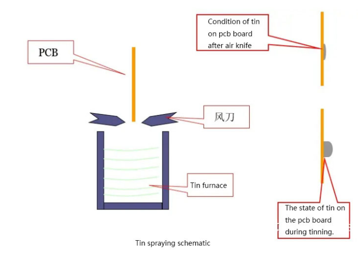
Before performing HASL surface finish, the PCB needs to be cleaned, usually through a micro-etching process to clean the copper surface. After cleaning, the PCB is preheated and coated with flux. The flux reduces surface tension between the PCB and solder, allowing the solder to better cover the PCB. Once flux is applied, the PCB is immersed in molten tin/lead solution, which covers the exposed copper pads and forms a tin-lead layer. After forming the tin-lead layer, high-pressure hot air knives are used to remove excess solder from the PCB surface and holes, ensuring uniform solder deposition, and leaving a thin, even protective layer on the pads.
Key parameters of the HASL process include solder temperature, dip time, air knife pressure, air knife angle, air knife distance, and PCB rise speed:
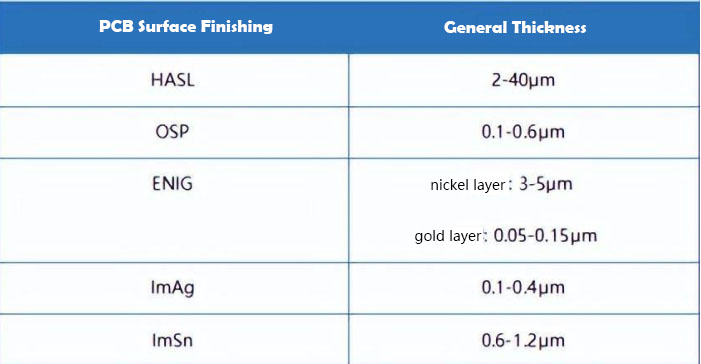
3. Comparison of HASL with Other PCB Surface finish Processes
Advantages of HASL:
1. Excellent solderability: The uniform solder layer formed by the HASL process ensures superior solderability. This even layer melts and flows more easily during soldering, creating reliable joints and improving the reliability of component connections. HASL is particularly well-suited for traditional through-hole components and some surface-mount devices.
2. Cost-effectiveness: Compared to other surface finish processes such as Electroless Nickel Immersion Gold (ENIG) or electroplated gold, HASL is more cost-effective. This lower cost makes HASL a practical choice for mass production, especially in cost-sensitive projects. Manufacturers can achieve reliable soldering and electrical performance without significantly increasing costs.
3. Wide application: HASL is suitable for most general-purpose PCB applications, covering sectors like consumer electronics and industrial equipment. Its mature process is easy to control and implement, meeting various design needs. Though not ideal for high-density or high-precision applications, HASL remains a preferred choice for many traditional applications.
Disadvantages of HASL:
1. Uneven thickness: A major drawback of HASL is the potential for uneven solder thickness, which is particularly problematic for high-density PCBs where fine-pitch components require precise solder thickness to avoid defects like bridging or opens, negatively affecting overall PCB performance.
2. Thermal stress: The high temperatures involved in HASL can cause thermal stress on the PCB substrate, leading to board warping, especially with thinner PCBs. This warping can result in assembly issues or degraded electrical performance. Care must be taken when working with heat-sensitive materials or thin substrates.
3. Environmental concerns: Traditional HASL uses lead-based solder, which poses potential risks to the environment and human health. Despite the introduction of lead-free HASL, lead-based processes are still used in many regions. With increasing environmental regulations, manufacturers must consider HASL's environmental impact and may need to seek alternatives to meet regulatory requirements.
4. Leaded vs. Lead-Free HASL: How to Choose?
In PCB manufacturing, HASL is a common surface finish process. However, with increasing environmental regulations, manufacturers are faced with the challenge of choosing between leaded and lead-free HASL. Below is a comparison of the two processes to help you make informed decisions during design and manufacturing.
Leaded HASL: Maintaining the Traditional Process
Lead-Free HASL: Leading the Environmental Trend
Process Challenges: While offering clear environmental benefits, lead-free HASL also presents challenges. The higher melting point of lead-free solder requires higher soldering temperatures, which may increase thermal stress on the PCB, especially for thinner substrates. Additionally, manufacturers may need to adjust equipment and processes to accommodate lead-free materials.
When choosing between leaded and lead-free HASL, consider the following factors:
Conclusion
Leaded and lead-free HASL each have their own advantages and disadvantages, and the choice depends on your specific needs and market environment. As technology continues to advance and environmental awareness grows, lead-free HASL is becoming the mainstream choice. However, for certain applications, leaded HASL remains a viable option. By understanding the characteristics of both processes, you can better select the appropriate surface finish solution for your project.
Still, need help? Contact Us: support@nextpcb.com
Need a PCB or PCBA quote? Quote now
|
Dimensions: (mm) |
|
|
Quantity: (pcs) |
|
|
Layers: 2 |
Thickness: 1.6 mm |
|
|
|

 Printed Circuit Boards
 Surface

