
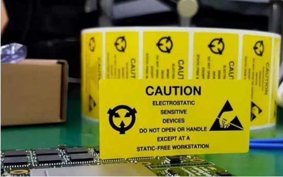
 PCB Assembly
 Layer Buildup
 Online Tools
 PCB Design-Aid & Layout
 Mechanics
 SMD-Stencils
 Quality
 Drills & Throughplating
 Factory & Certificate
 PCB Assembly Factory Show
Certificate
PCB Assembly Factory Show
Certificate
Support Team
Feedback:
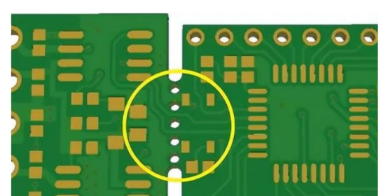
support@nextpcb.comMouse Bite Panelization refer to a series of small holes designed along the edge of a printed circuit board (PCB). These holes are arranged similarly to the perforations on the edge of a postage stamp, hence the name "stamp holes." This design allows for easy separation or detachment of multiple PCB boards. The name "stamp hole" originates from the resemblance to the perforated edge of a postage stamp.
Types of Mouse Bite :
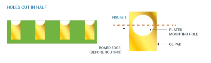
1、Half-hole: A common type of stamp hole characterized by a relatively small diameter, used for positioning and securing on the PCB.
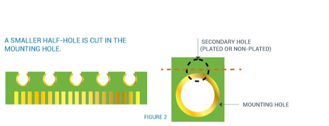
2、Smaller half-holes: A variation with even smaller diameters, ideal for applications requiring more precise positioning.
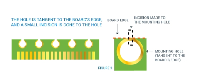
3、Edge-tangent holes: These holes are positioned close to the edge of the PCB and are typically used for specific connection or securing needs.
Different types of mouse bite serve distinct roles in PCB design. Selecting the appropriate type of stamp hole based on specific application requirements is key to ensuring the PCB functions reliably.
3. Common Design Techniques for PCB mouse bites
4. Difference Between PCB Stamp Holes and V-Cut
V-Cut: V-Cut is one of the most common methods for PCB panelization. It involves cutting V-shaped grooves between PCB boards, allowing for easy separation during or before packaging. Double-sided V-cuts are typically controlled to a depth of about one-third of the board thickness (the sum of both sides' grooves). Accurate control of groove size and depth is crucial to ensure easy separation without compromising the strength of the board.
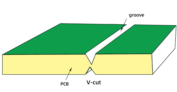
V-Cut
Use cases for V-Cut: It is suitable for linear-connected PCBs. V-Cut is simple to design and easy to handle, but the depth and width of the groove must be precisely controlled to allow for easy separation while maintaining the board's strength.
Advantages of stamp holes: mouse bites provide greater strength and can be broken off directly without the need for milling equipment. They are well-suited for irregularly shaped PCBs or applications requiring high precision. After detachment, the edges remain neat, similar to the edge of a postage stamp.
Summary
V-Cut is ideal for linear PCB panelization due to its simple design and ease of use, but the groove depth and width must be tightly controlled.
mouse bits offer better strength and are suited for irregular PCB shapes or applications requiring high precision. They can be broken manually without additional cutting equipment, making them more suitable for complex shapes and ensuring cleaner edges after separation.
Still, need help? Contact Us: support@nextpcb.com
Need a PCB or PCBA quote? Quote now
|
Dimensions: (mm) |
|
|
Quantity: (pcs) |
|
|
Layers: 2 |
Thickness: 1.6 mm |
|
|
|

 Printed Circuit Boards
 Surface

