

 Printed Circuit Boards
 Surface
 PCB Assembly
 Layer Buildup
 Online Tools
 PCB Design-Aid & Layout
 Mechanics
 SMD-Stencils
 Quality
 Drills & Throughplating
 Factory & Certificate


|
Aspect |
Circuit Board |
Printed Circuit Board (PCB) |
|
Definition |
A broad term encompassing various types of circuit boards |
Specifically refers to boards made via printing techniques |
|
Manufacturing Method |
Can be created through manual wiring or soldering |
Produced through chemical etching and printing processes |
|
Conductive Pathways |
Manually connected or wired |
Etched copper paths form the circuit layout |
|
Component Mounting |
Typically involves manual component placement |
Supports both THT and SMT mounting techniques |
|
Application |
Used in prototypes, small-scale production, or early electronics |
Common in modern electronics and mass production |
What Files Are Required for PCB Manufacturing
When preparing for PCB manufacturing, it’s essential to provide a set of specific files and documents to ensure a smooth production process. These files communicate your design intent to the manufacturer and ensure that the final product matches your specifications. Here are the key files required:
1. Gerber Files
Gerber files are the most critical files used in PCB manufacturing. They define the PCB's layer structure, copper traces, pads, holes, and other essential design features. These files are essentially a blueprint of the PCB and include information for each layer of the design, such as:
- Copper layers: Top and bottom signal layers, inner layers (for multi-layer PCBs).
- Solder mask: Defines areas to be coated with solder mask to prevent soldering in certain areas.
- Silkscreen: Markings for component placement, logos, and other symbols.
- Drill files: Locations and sizes of holes for vias, components, and mounting. Gerber files are the primary format used by manufacturers to fabricate the PCB.
Why gerber files are important for manufacturing
Manufacturers typically need the original Gerber files for adjustments and optimization. For example, if your original design has a line width of 6mil, but the file you send to the supplier shows a width of 6.6mil, this modified file is referred to as a "working Gerber" (used for production). Such files have been processed through CAM, potentially including manufacturing compensation, process optimization, and other necessary adjustments. Given that each manufacturer has its own engineering workflow, they may find these changes unclear.
- Original Gerber File: The file generated during the design phase, containing the designer's initial intent and all design details.
- Working Gerber File: This file has undergone processing and adjustment, including pre-production compensation and optimization.
- Why Factories Need Original Files: To ensure that all compensations and optimizations are correctly applied, manufacturers usually require the original design Gerber file. This helps prevent confusion or problems that may arise due to unclear modifications in the working files.
This article will help you understand gerber: what is gerber file? how to create gerber file? how to open gerber file? how to import gerber file from Kicad/Altium/Diptrace/ Eagle? Gerber Files for PCBs: Creating, Viewing, Converting and Manufacturing Relationship
2. Drill Files
Drill files contain information about all the holes that need to be drilled in the PCB. This includes the location, size, and type of hole (e.g., through-holes, vias, or blind/buried vias). Drill files are essential for defining the holes used for component leads, vias for electrical connections between layers, and mounting holes for securing the PCB in an enclosure.
3. Layer Stack-up
The Layer Stack-up document defines the arrangement and material specifications for each layer of a multi-layer PCB. It specifies the sequence of the layers, their thicknesses, and the type of materials used. This information is essential for the manufacturer to correctly build the PCB, ensuring it meets electrical, mechanical, and thermal requirements. For a multi-layer PCB, the Layer Stack-up typically includes:
- Layer Sequence: The order of layers (e.g., top layer, inner signal layers, ground/power planes, bottom layer).
- Material Types: The materials used for each layer, such as FR4, copper, or other laminates.
- Layer Thickness: The thickness of copper, prepreg, and core materials, which is important for controlling impedance and ensuring signal integrity.
- Impedance Control: Details on how the stack-up maintains specific impedance for high-speed designs.
Once these files are submitted to the PCB manufacturer, they will conduct a thorough review to ensure that the design is optimized for manufacturability and assembly, and that no errors exist in the production process.
PCB Manufacuring Process
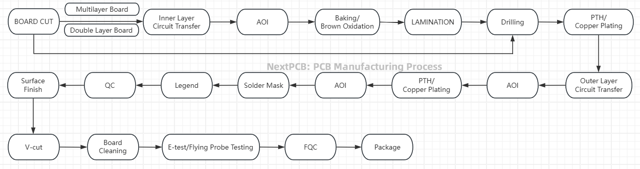
the pcb manufacturing process flowchart
The PCB manufacturing process demands strict requirements, involving multiple complex steps to ensure the final product's quality, performance, and reliability. Multilayer boards offer higher integration and more complex circuit designs. Below is the PCB manufacturing process for multilayer PCBs, covering all stages from raw materials to finished products.
Step 1. Board Cut
According to the requirements of designs, cut the substrate material into the required size for the work. The following issues need attention:
- To avoid burrs on the edges affecting quality, perform edge grinding and rounding after cutting.
- Consider shrinkage effects and bake the boards before proceeding to the next process after cutting.
- Ensure that the cutting aligns with the warp and weft directions as per engineering specifications to prevent warping and other issues.
Step 2. Inner Layer Circuit Transfer
2.1 Surface Treatment/Grinding
Remove contaminants from the copper surface and increase its roughness to facilitate the subsequent lamination process.
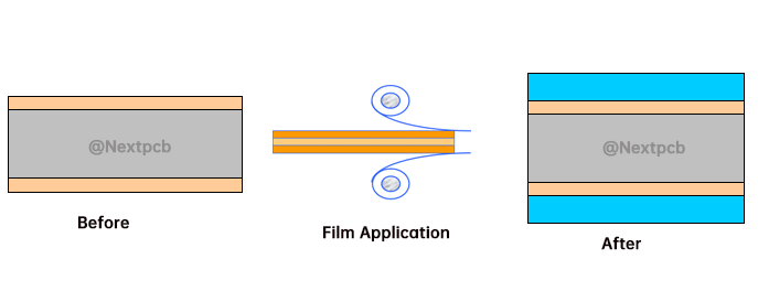
2.2 Film Application
A photosensitive film is applied to the treated substrate in preparation for exposure.
Common Issues and Solutions in Film Lamination
a. Bubbles Between Dry Film and Copper Foil Surface
Solution: Selecting smooth copper foil is crucial. To reduce bubbles, increase lamination pressure and handle the boards gently. Regularly inspect and maintain the smoothness of the hot press rollers to prevent dents and contamination from the film. Additionally, lowering the lamination temperature can help avoid material wrinkling due to temperature differences.
b. Poor Adhesion of Dry Film on Copper Foil
Solution: Inadequate cleaning of the copper foil surface can leave oil residues or oxidation layers. Always wear gloves when handling boards to ensure cleanliness. Using high-quality dry film and regularly checking its expiration date are also critical. Adjusting lamination speed and temperature while maintaining relative humidity around 50% in the production environment can enhance dry film adhesion.
c. Wrinkling of Dry Film
Solution: Excessive stickiness of the dry film can lead to wrinkling during handling. Careful placement of the boards and prompt resolution of any contact issues are necessary. Additionally, reducing the preheating temperature of the boards can help mitigate the risk of wrinkling.
d. Residual Adhesive Issues
Solution: Residual adhesive problems may stem from poor-quality dry film, excessive exposure time, or ineffective developer solution. To address these issues, switch to high-quality dry film, adjust the exposure time, and replace the developer solution with a new one.
2.3 Exposure
The inner layer circuit pattern is transferred onto the photosensitive film using exposure equipment. Areas not exposed to light will be removed in the developing stage. When performing PCB pattern exposure, the following aspects need to be considered:
a. Proper Exposure Time
Exposure time refers to the duration for which the PCB is illuminated in the exposure equipment. Both excessively long and short exposure times can adversely affect the PCB. An overly long exposure time can result in excessive light intensity, causing the conductive layers on the circuit board to lose adhesion or even burn out. Conversely, too short an exposure time may prevent the photoresist layer from fully curing, thereby affecting the insulation performance of the circuit board. Therefore, exposure time should be set appropriately based on the requirements of the PCB design and the characteristics of the exposure equipment.
b. Appropriate Exposure Distance
Exposure distance is the distance from the light source to the PCB, which significantly impacts the exposure effect. A too short exposure distance can subject the circuit board to excessive light intensity, leading to issues such as melting or deformation of the board surface. On the other hand, an excessively long exposure distance can reduce the exposure effectiveness, preventing the photoresist layer from curing adequately. Thus, selecting an appropriate exposure distance is crucial for ensuring effective exposure.
c. Strict Control of Temperature and Humidity
The temperature and humidity during the PCB exposure process are also critical factors that require strict control. A high-temperature environment can cause the photoresist layer to deform due to heat, thus affecting the manufacturing accuracy of the PCB. Excessive humidity can lead to moisture absorption in the photoresist layer, causing it to soften and lose adhesion. Therefore, it is essential to maintain temperature and humidity within suitable ranges during PCB exposure to ensure the quality and adhesion of the photoresist layer.
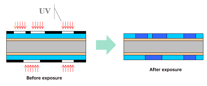
PCB graphic exposure diagram
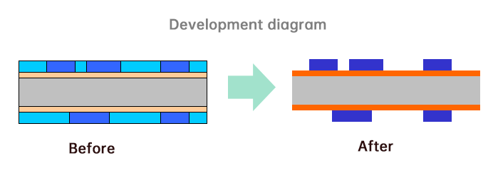
2.4 Development
The unexposed areas of the photosensitive film are removed using a developer solution, revealing the circuit pattern. During the PCB manufacturing process, several common issues may arise during the development stage, including the following:
Incomplete Development: Incomplete development can result from multiple factors. For instance, excessive pre-bake temperature or duration may cause the solder mask to become "cooked", making it difficult for the developer to remove the unexposed areas. Additionally, high exposure energy, inadequate vacuum pressure, insufficient film opacity, improper development parameter settings, unsuitable temperature and humidity in the cleanroom, and extended time between silkscreen printing and pre-baking can all negatively affect development, leading to incomplete results.
Dry Film Delamination: Dry film delamination refers to the separation between the dry film and the substrate. This issue often arises due to improper surface treatment of the substrate, which can reduce the adhesion between the dry film and the substrate. Other contributing factors may include uneven copper foil coating, insufficient thermal pressing, ink contamination, and prolonged storage.
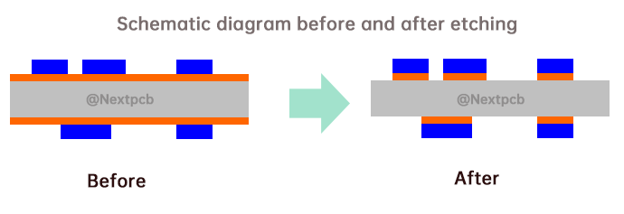
2.5 Etching
A chemical etching process is employed to remove the unprotected copper, forming the desired circuit pattern.
The etching process of PCB is a crucial stage in electronic manufacturing that directly impacts the precision of conductor patterns and the performance of the final product. To enhance the success rate of PCB etching, it is essential to adhere to the following key considerations:
Control of Side Etching and Edge Accumulation
- Optimize Etching Method: Utilize a spray etching method to reduce side etching, which is more effective than immersion, bubbling, or splashing techniques.
- Select Appropriate Etchant: Choose etchants with a high etching coefficient based on actual needs, such as alkaline copper chloride or experimental nitric acid-based etching systems, to minimize side etching risks.
- Control Etching Rate: Increase the etching rate to shorten the PCB's exposure time in the etching solution, effectively reducing side etching.
- Adjust Etchant Parameters: Ensure the pH of the etching solution remains within an appropriate range (e.g., for alkaline etchants, pH should be kept below 8.5), and maintain moderate density in the etching solution, favoring optimal copper concentration.
- Choose Suitable Copper Foil: For etching fine traces, use ultra-thin copper foil and adjust the thickness according to the trace width to minimize side etching.
Control of Pre-Processing Steps
Ensure thorough de-masking by reinforcing the pre-processing step to prevent residual film from contaminating the etching solution and causing sludge formation, which could impair etching quality. Special attention should be paid to the treatment of edge masks and over-plating.
Mitigate Contamination Issues
Copper contamination of water is a common issue in PCB production, exacerbated by the use of ammonia-based etchants. Due to the complex formation of copper with ammonia, it is challenging to remove using ion exchange or alkaline precipitation methods. It is recommended to implement a second spray operation using copper-free additives to rinse the PCB, significantly reducing copper discharge. Prior to water rinsing, use an air knife to remove excess solution from the board surface, thereby alleviating the rinsing burden on the water with respect to copper and etching salts.
2.6 Film Removal/Stripping
The remaining photosensitive film is removed, completing the manufacturing of the inner layer circuit. In the PCB film stripping process, the primary reasons for incomplete stripping can be summarized as follows:
- Ineffective solvent: If the chemicals used are not strong enough, the photoresist may not dissolve completely, resulting in incomplete delamination.
- Improper solvent ratio: If the solvent ratio is too concentrated or too diluted, it can adversely affect its dissolving effectiveness, leading to incomplete delamination.
- Incomplete etching: If the etching process is not thorough, residual photoresist can interfere with the subsequent delamination process.
- Water quality issues: Excessive impurities or poor-quality water can disrupt the cleaning process, negatively impacting the quality of the delamination.
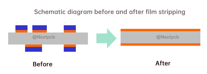
Schematic diagram of PCB stripping
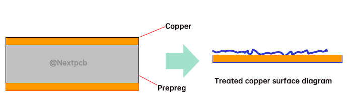
Step 3. Baking/Brown Oxidation
Thermal treatment is applied to stabilize the structure of the inner layer circuit board and enhance its durability.
Main Functions of PCB Brown Oxidation:
- Enhanced Bonding Strength: The brown oxidation process significantly improves the bonding strength between the inner core substrate and the prepreg by creating a uniform fibrous structure, preventing delamination and board explosion issues.
- Improved Surface Cleanliness: This process effectively removes oils and contaminants from the surface, ensuring a clean board that provides a solid foundation for subsequent processes.
- Copper Surface Roughening: By roughening the copper surface, brown oxidation increases the bonding area and surface adhesion, thereby enhancing structural stability.
- Corrosion and Oxidation Resistance: Brown oxidation effectively reduces the oxidation rate of the copper surface, minimizing exposure to air and moisture, which extends the lifespan of the PCB.
- Enhanced Reliability and Aesthetic Appeal: During the brown oxidation process, oxides fill surface defects, shortening the distance between copper and joining metals, improving conductivity and overall reliability. Additionally, the deeper color and texture enhance the board's aesthetic appeal, aligning with modern design standards.
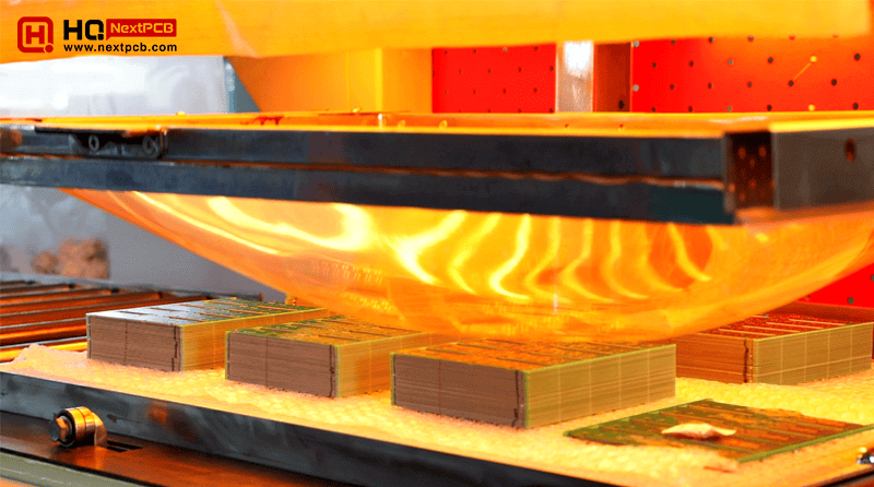
Step 4. Lamination
The inner layers of the circuit boards are pressed together using a laminating machine to form a cohesive structure.
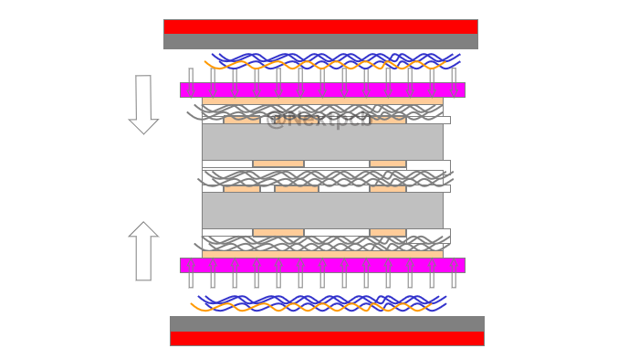
Pressing the laminated boards into multilayer boards using a hot pressing method
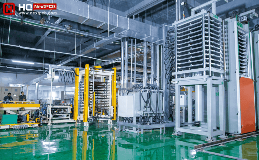
Lamination machines from NextPCB
Common Issues in PCB Lamination Process
- Board Deformation: Deformation is a frequent issue during lamination, often caused by inadequate pre-treatment, uneven temperature or pressure, or material design flaws. Deformed boards affect machining accuracy and can lead to unreliable electrical connections.
- Bubbles and Voids: Bubbles and voids compromise electrical performance and mechanical strength, usually due to trapped air or uneven resin flow.
- Resin Loss and Excess Resin: Resin loss can weaken adhesion, while excess resin can contaminate surfaces, affecting soldering and assembly. These issues relate to resin quantity, viscosity, and lamination conditions.
- Misalignment Issues: Precise alignment of layers in multilayer PCBs is crucial; misalignment can lead to electrical failure or performance degradation.
- Residual Stress and Cracking: Temperature and pressure changes during lamination can induce residual stress, leading to cracking or performance degradation later.
Step 5. Drilling
Precision drilling is performed on the laminated board to prepare for subsequent plating and connections.
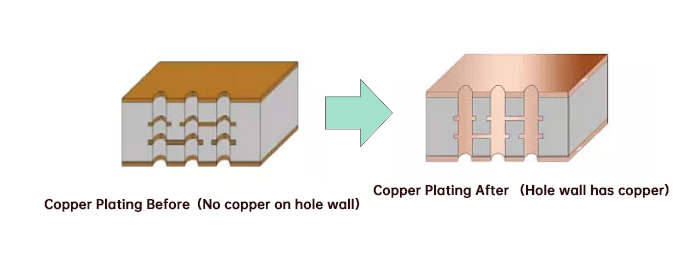
Step 6. PTH/Copper Plating
In the PCB manufacturing process, the pcb plating typically begins with sinking copper , also known as Plated Through Hole (PTH). The purpose of sinking copper is to deposit a layer of 0.3 to 0.5 micrometers of copper inside the holes using a chemical reaction involving formaldehyde in a strongly alkaline potassium permanganate environment. This process transforms the initially non-conductive drilled holes into conductive pathways, facilitating subsequent board electroplating and graphic plating to achieve the required thickness as specified by the customer. Following the sinking copper process, there are another two copper platings:
- First Copper Plating: A thickness of 200-500 microinches of copper is plated over the chemically sinking copper, which is only 20-40 microinches thick. This step protects the chemical copper from damage during subsequent processes, preventing hole breakage.
- Second Copper Plating: After development, additional copper is plated on the exposed copper surface to achieve the desired thickness as specified by the customer. This happens after the Outer Layer Pattern Plating.
- Additionally, tin plating may be performed. A layer of tin is applied after the second copper plating to protect the surface during the etching process.
Step 7. Outer Layer Dry Film
A photosensitive film is applied to the outer copper surface in preparation for exposure. Similar to the inner circuit.
Step 8. Outer Layer Pattern Plating
The exposure, development, and etching processes are repeated for the outer layer circuit to form the desired pattern. Similar to the inner circuit.
Step 9. Solder Mask
A solder mask is applied over the circuits to prevent short circuits during the soldering process. Solder mask serves as an essential protective layer with the following purposes:
- Prevention of Short Circuits: The solder mask covers all traces and copper surfaces while leaving only the vias and pads exposed, effectively preventing short circuits during wave soldering and reducing solder consumption.
- Circuit Protection: The solder mask protects the circuitry from moisture and various electrolytes that can cause oxidation, thereby safeguarding electrical performance. It also prevents mechanical damage from external sources, maintaining good insulation.
- Enhanced Insulation: As PCBs become thinner and trace widths decrease, insulation issues between conductors become more pronounced. The insulation properties of the solder mask are crucial in preventing short circuits.
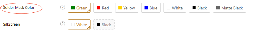
- Aesthetic Improvement: The solder mask is typically green or available in other colors, enhancing the PCB's visual appeal to meet modern aesthetic standards.
- Identification and Marking: Markings on the solder mask assist in identifying component locations and functions, facilitating assembly and maintenance.
Solder mask is usually green, but there are other colors to choose from, and the functions are the same, the following are the solder mask color options listed in the PCB online quote options supported by Nextpcb:
Step 10. Silkscreen Printing
Identifiers, characters, and other necessary information are printed on the PCB surface.
Step 11. Surface Treatment/ Finish
Surface treatments is also commonly referred to as Surface Finish. In conventional PCBs, copper layers are present on the substrate. If these copper layers are unprotected, they can oxidize and degrade, adversely affecting subsequent soldering processes. Various protective layers can be applied, with the most common types including: Hot Air Solder Leveling (HASL), Organic Solderability Preservative (OSP), Electroless Nickel Immersion Gold (ENIG), Nickel-Gold plating, Gold Fingers, Immersion Silver (IS), and Immersion Tin (IT).
Hot Air Solder Leveling (HASL)
After the board is fully covered with solder, excess solder is removed using high-pressure hot air, leveling the solder on pads and hole walls, with options available for both leaded and lead-free versions. This process offers the advantages of low cost and sustained solderability throughout the manufacturing process.
Organic Solderability Preservative (OSP)
A thin, uniform protective layer is applied to the copper surface of the PCB, offering advantages such as comparable cost to HASL, good coplanarity, and a lead-free process.
Electroless Nickel Immersion Gold (ENIG)
Nickel is deposited on the copper surface through a chemical reaction, followed by a layer of gold, providing excellent solderability, a smooth surface, a long shelf life, and the ability to withstand multiple reflow soldering processes.
Nickel-Gold Plating
Nickel and gold are electroplated onto the copper surface, offering good solderability, a flat surface, long storage life, and durability during multiple reflow soldering processes.
Gold Fingers
Nickel and gold are electroplated onto the contact surfaces of connectors, offering enhanced conductivity and durability.
Immersion Silver (IS)
A metal layer of 0.1 to 0.6 micrometers of silver is deposited onto the copper layer for protection, providing good solderability, a smooth surface, and serving as a natural alternative to HASL.
Immersion Tin (IT)
A metal layer of 0.8 to 1.2 micrometers of tin is deposited onto the copper layer for protection, offering good solderability, a smooth surface, and relatively low cost.
What is the difference between different PCB Surface Finish
| Surface Finish Type | Advantages | Disadvantages |
|
HASL (Hot Air Solder Leveling) |
- Low cost, suitable for mass production | - Not environmentally friendly (traditional HASL contains lead, which is not RoHS-compliant); Lead-free HASL is more expensive |
| - High reliability, suitable for conventional soldering | - High reliability, suitable for conventional soldering | |
|
ENIG (Electroless Nickel Immersion Gold) |
- Excellent solderability, ideal for high-density and fine-pitch packages (e.g., BGA, CSP) | - Higher cost |
| - Strong corrosion resistance, prevents copper oxidation | - Gold layer can become brittle at high temperatures | |
| - Good flatness, suitable for precision soldering | - Non-uniform gold layer thickness may affect surface quality | |
|
OSP (Organic Solderability Preservative) |
- Environmentally friendly (lead-free), RoHS compliant | - Not suitable for high-temperature applications, poor high-temperature performance |
| - Low cost, fast production | - Poor solderability, not suitable for high-density or fine-pitch soldering | |
| - Low environmental requirements, ideal for small-volume production | - Poor durability, oxidizes over time when exposed to air, causing loss of protection | |
| Immersion Silver | - Excellent solderability, ideal for precision soldering | - Silver layer is prone to sulfurization, especially in humid environments, affecting long-term reliability |
| - Environmentally friendly, RoHS compliant | - Relatively high cost | |
| - Strong corrosion resistance, ensures electrical performance | - Thin silver layer may wear out, affecting performance over time | |
| Immersion Tin | - Excellent solderability, ideal for precision soldering | - Tin layer thickness may vary, affecting soldering quality |
| - Environmentally friendly, RoHS compliant | - Tin layer is prone to oxidation, which may reduce soldering performance over time | |
| - Moderate cost, suitable for general applications | - Limited applicability, especially in high-density packages | |
| Electrolytic Nickel & Gold | - Excellent solderability, suitable for high-density packages | - Higher cost |
| - Strong corrosion resistance, excellent protection | - Thick gold layer may become brittle over time, affecting long-term reliability | |
| - Provides uniform nickel-gold layers, ideal for high-performance applications | - Complex process may increase production time and cost |
Step 12. Shaping
The PCBs are cut into their final shapes to meet customer requirements.
Step 13. Electrical Testing
The produced PCBs undergo electrical testing to ensure that all circuits are connected properly and meet design specifications.
Step 14. Final Inspection
A comprehensive inspection is performed on the PCBs, including appearance, dimensions, and electrical performance, to ensure product quality.
Step 15. Packaging
Finally, qualified PCBs are appropriately packaged to prevent damage during transportation and storage. For bare boards, vacuum packaging is generally sufficient, with additional anti-collision measures.
Vacuum packaging
In conclusion, the PCB manufacturing process involves numerous complex steps, especially when dealing with multilayer boards and specialized techniques. Each stage is critical, as any oversight can significantly impact the functionality of the final PCBA. NextPCB offers free online Gerber Viewer inspections and DFM checks, along with verified working Gerber files, all aimed at safeguarding quality. Our commitment to quality first is paramount throughout the production process.
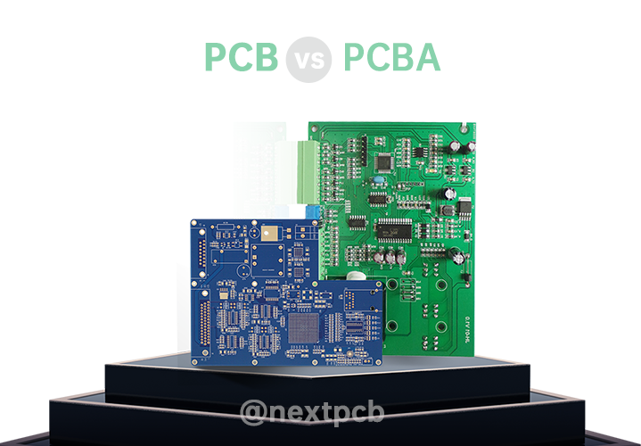
What is PCBA?
PCBA, or Printed Circuit Board Assembly, refers to the process of mounting and soldering various electronic components onto a PCB. A PCBA represents a fully assembled and functional circuit module that is capable of executing specific electronic functions. Unlike a PCB, which is merely a bare board, a PCBA is a complete unit that has undergone assembly, soldering, and testing.
Components of a PCBA:
- PCB (Printed Circuit Board): The foundation of a PCBA is the PCB itself.
- Electronic Components: These include resistors, capacitors, IC chips, diodes, and other components that are mounted onto the PCB using automated or manual methods.
- Solder Paste : Solder Paste is used to secure the components, creating a solid electrical connection between component leads and PCB pads.
What Files Are Required for PCB Assembly Manufacturing
BOM (Bill of Materials)
The BOM is a detailed list of all the components used in PCB assembly. It not only lists the part numbers, specifications, and quantities of each component but also includes unique identifiers, supplier information, and other relevant details.
If you plan to calculate prices online, each distributor may have different BOM format requirements. Therefore, when selecting a suitable and reliable supplier, it is important to ensure that the BOM file format is compatible with their online pricing system. Obtain NextPCB's BOM file template to quickly evaluate your BOM quote online.
Gerber Files
Gerber files are a standard file format used to describe all the design information for a PCB, including layer structure, copper patterns, pads, hole locations, and more. These files serve as the foundational documents for PCB manufacturing and assembly.
Centroid Files
Centroid files are typically used in automated placement processes. They provide detailed information on the precise locations, rotation angles, and pickup points for each component on the PCB.
Once these documents are provided, NextPCB will conduct a thorough review based on the materials submitted. This includes evaluations such as DFA (Design for Assembly) audits to ensure that the design is optimized for efficient assembly and meets manufacturability standards.
Learn more about How to Create a Centroid(Pick and Place) File Instantly?
HQDFM: Free PCB Design Analysis Tool with over 50 DFM and DFA Checks
PCB Assembly (PCBA) Process
In modern electronics manufacturing, the surface mount production process is crucial for ensuring the efficiency and reliability of electronic products. Below is a detailed description of the surface mount production process along with key considerations for each stage.
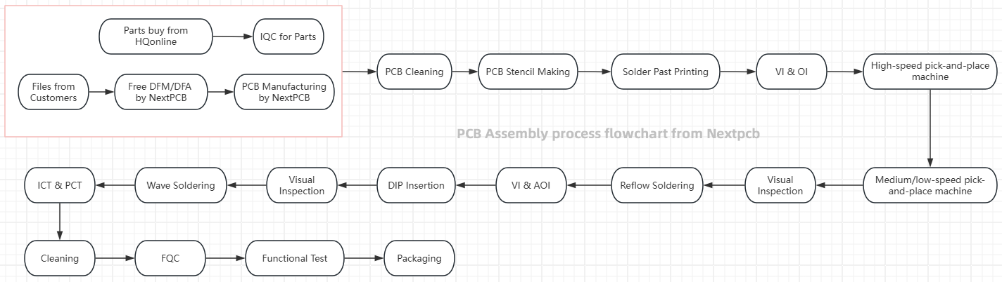
PCB assembly process flowchart
Step 1. HQonline Component Procurement
The first step in the PCB assembly process is ensuring that the required components meet the specifications and quantities outlined in the design. It is essential to choose reliable suppliers and confirm delivery dates to prevent production delays.
Step 2. Incoming Quality Control (IQC)
Upon receiving components, a comprehensive incoming material inspection is necessary. This includes verifying the quantity, type, and quality of components to ensure there are no defects. Additionally, implementing Electrostatic Discharge (ESD) protection measures is critical to safeguard the components from damage.
Step 3. PCB Cleaning
Cleaning the PCB is a key step in ensuring the quality of subsequent soldering processes. Appropriate cleaning agents and methods should be employed to remove oils and dust, which can adversely affect solder paste printing and soldering quality.
Step 4. PCB Stencil Making
The design of the stencil must be accurate, with hole sizes and spacing matching the pads on the PCB to ensure uniform solder paste application. Care should be taken to avoid any defects during the fabrication process.
Step 5. Solder Paste Printing
The quality of solder paste printing directly impacts soldering effectiveness. The thickness and uniformity of the solder paste must be controlled to avoid under- or over-printing. Additionally, the use of the appropriate squeegee pressure is essential.
Solder paste management is a critical aspect of the SMT process, requiring strict control to ensure quality.
- The paste must be refrigerated at a temperature between 0-10°C when not in use,
- The container should always be sealed tightly.
- Solder paste should not remain on the stencil for more than 0.5 hours to prevent degradation.
- Before use, it must be brought to room temperature for at least 2 hours and stirred for 3-5 minutes in the same direction using a tool with rounded edges to avoid damaging the solder balls.
- The paste must be consumed within 24 hours of opening to maintain its effectiveness.
Step 6. Visual Inspection/Optical Inspection
After solder paste printing, a visual inspection or optical inspection should be conducted to ensure the completeness and uniformity of the solder paste on the pads, laying the groundwork for the subsequent component placement.
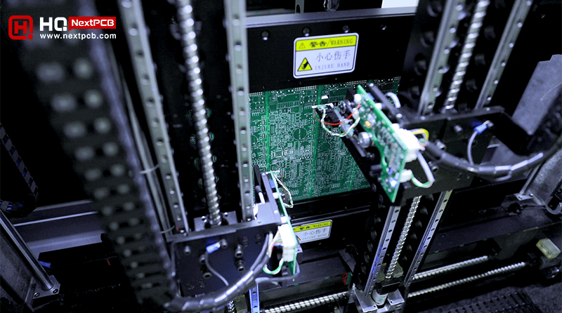
Step 7. High-Speed Pick-and-Place Machine Operation
High-speed pick-and-place machines are utilized for precise component placement. It is vital to ensure that the machine settings are correct and that the orientation and position of the components are accurate to avoid misplacement.
● High-speed machines typically feature 10 to 15 placement heads, with each head capable of swapping 2 to 5 nozzles for different components.
● The components are picked up using vacuum suction technology.
● The placement speed is around 10 components per second.
● Depending on the cycle time of the bottleneck workstation, 1 to 3 machines are usually installed per SMT production line.
● High-speed machines can experience material wastage (component misfeeds), particularly with loose or scattered parts. Therefore, during the sample production phase, it's recommended to prepare extra components. A buffer of around 10 additional pieces beyond the actual production count is advisable to account for such wastage.
Step 8. Medium to Low-Speed Pick-and-Place Machine Operation
Following high-speed placement, a medium to low-speed pick-and-place machine is used for smaller components, requiring similar attention to accuracy.
For general-purpose pick-and-place machines, they typically feature 3 to 5 placement heads, each capable of swapping 2 to 5 nozzles. These machines can place 1 to 2 components per second from tape reels and take 1 to 3 seconds for components from trays. Generally, each SMT production line is equipped with one of these machines.
Step 9. Pre-Reflow Inspection
Before reflow soldering, a pre-reflow inspection is performed to check the integrity of all placed components, ensuring there are no loose or incorrectly positioned parts.
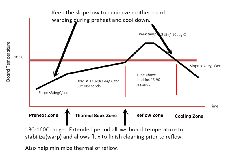
Step 10. Reflow Soldering
Reflow soldering is a critical step that requires the appropriate temperature profile to be set. It is important to avoid overheating or poor cooling of solder joints to prevent defects.
The temperature profile is critical during the reflow soldering process. It is typically divided into four zones: the preheat zone, thermal soak zone, reflow zone, and cooling zone. Each zone has specific temperature control requirements to ensure the quality of the solder joints and the reliability of electronic components.
- 1. When the PCB enters the preheat zone, the solvents and gases in the solder paste evaporate. At the same time, the flux in the solder paste begins to wet the pads, component terminals, and leads. The solder paste softens, collapses, and covers the pads, isolating them from oxygen.
- 2. As the PCB enters the thermal soak zone, it is preheated thoroughly to prevent damage to the PCB and components from a sudden rise in temperature when entering the reflow zone.
- 3. When the PCB reaches the reflow zone, the temperature rises rapidly, causing the solder paste to melt. The liquid solder wets, diffuses, and flows over the pads, component terminals, and leads, forming a solid solder joint.
- 4. Finally, the PCB enters the cooling zone, where the solder joints solidify, completing the reflow soldering process.
Step 11. Visual Inspection and Automated Optical Inspection (AOI)
After soldering, visual inspection and AOI are performed to confirm the quality of solder joints and to identify and rectify any soldering defects promptly.
Common Issues in PCBA Reflow Soldering:
Cold Solder Joint: The solder joint appears visually acceptable but does not actually contact the component leads or pads. This defect may occur due to insufficient melting of the solder or inadequate wetting of the soldering area. Components with cold solder joints may fail to establish electrical connections, resulting in functional failure.
- Solder Bridging: Excess solder appears between component leads, causing a short circuit.
- Dry Joint/Cold Solder: The solder joint is not secure and may result from insufficient temperature or inadequate soldering time, leading to poor electrical contact.
- Component Misalignment: Components may shift during the soldering process, resulting in incorrect positioning.
- Solder Balls: Small solder balls may form during the soldering process, posing a risk of short circuits.
- Missing/Incorrect Components: Certain components may not be correctly placed or may be replaced with incorrect components.
- Poor Solder Joint: The solder joint may be excessively large or small, or its shape may be irregular, potentially affecting electrical performance.
Step 12. DIP Insertion
For through-hole components, it is crucial to ensure correct orientation and proper insertion depth. Checking the insertion depth is vital for ensuring soldering quality.
Considerations During the DIP Insertion Process
- Maintain Cleanliness: Before insertion, check the surfaces of electronic components for contaminants such as grease or paint. Ensuring that the surfaces are clean is crucial to avoid compromising the quality of insertion and soldering.
- Flat Placement and Orientation: During the insertion process, ensure that the electronic components are flat against the PCB. After insertion, verify that the components are level and not uneven. Additionally, components with directional indicators must be inserted according to their specified orientation to prevent incorrect placement.
- Avoid Obstructing Pads: Ensure that the inserted leads do not obstruct the pads to guarantee the quality and reliability of soldering.
- Control Insertion Force: Be mindful of the force applied during insertion to avoid excessive pressure that could damage the components or the PCB.
- Height and Spacing: When inserting electronic components, ensure they do not exceed the edges of the PCB, paying particular attention to the height of the components and the spacing between them.
Step 13. Visual Inspection
After DIP insertion, another visual inspection should be conducted to ensure that there are no defects in the solder joints of the inserted components, thereby guaranteeing product reliability.
Step 14. Wave Soldering
Wave soldering is used for handling through-hole components, requiring appropriate soldering parameters to be set to ensure uniform soldering and to avoid cold solder joints.
Detailed Process of Wave Soldering
- Pre-treatment: Before wave soldering, the PCB must undergo cleaning and pre-treatment to remove surface oils, dust, and other contaminants, ensuring soldering quality.
- Component Placement: Accurately place the DIP components on the PCB.
- Flux Application: Apply flux evenly in the soldering area of the PCB. Prior to soldering, a layer of flux (rosin or other flux agents) needs to be applied to the PCB to prevent bridging or cold soldering during the soldering process.
- Wave Soldering Machine Preparation: Insert the prepared PCB into the wave soldering machine. The wave soldering machine typically consists of several main components, including the preheating zone, solder pot, and cooling zone.
- Preheating Phase: The PCB passes through the preheating zone, where the temperature gradually increases to remove moisture from the PCB, flux, and components. This phase also helps reduce the temperature differential between the PCB and the components, preventing thermal stress damage.
- Soldering Phase: The PCB travels through the solder pot of the wave soldering machine, where it encounters a wave of molten solder. The height and temperature of the solder wave are precisely controlled to ensure that the solder adequately wets the component leads and PCB pads, forming strong solder joints. During the soldering process, the underside of the PCB makes contact with the solder wave, allowing the leads to be fully immersed in the solder, thus achieving soldering.
- Hot Air Knife: After soldering, a hot air knife is used to blow away excess solder, resulting in smoother and more uniform solder joints.
- Cooling Phase: The PCB passes through the cooling zone, allowing the solder joints to cool and solidify quickly, ensuring the strength and reliability of the joints.
- Post-treatment: After completing the wave soldering process, the soldered PCB must be inspected. This includes trimming the edges of the assembled PCBA to the appropriate size and conducting visual inspections and Automated Optical Inspections (AOI) to detect solder defects, such as cold solder joints and shorts. Any incomplete soldered PCBA boards may require rework and repairs.
Learn more about How does Wave Soldering Mastery work in PCBA by:
Step 15. In-Circuit Testing (ICT) and Product Conformance Testing (PCT)
In-circuit testing (ICT) and product conformance testing (PCT) are performed to ensure that the electrical functionality of the circuit is normal and that the product meets design specifications.
Step 16. Cleaning
After soldering, the PCBs should be cleaned using appropriate methods to remove flux residues and other contaminants, preventing corrosion.
Step 17. Final Quality Control (FQC)
A comprehensive final quality control check is necessary to ensure that all products meet quality standards, and the inspection results should be documented.
Step 18. Functional Testing
Functional testing is conducted on the PCBs to ensure all functionalities operate correctly and that all parameters meet design requirements. Including but not limited to the following:
- Electrical Connectivity: Verify the electrical performance, including voltage, current, and power consumption.
- Communications: Confirm the reliability and correctness of communication interfaces (e.g., UART, I2C, SPI, USB, HDMI, Ethernet).
- Signal Integrity: Signal integrity and timing accuracy.
- Memory: Test the read and write functionality of RAM and flash memory.
- Functional Module Test: Evaluate the operation of various modules like buttons, LED indicators, and sensors.
- Clock Test: Check the frequency and stability of clock signals.
- Fault Detection and Fault Tolerance Test: Simulate fault conditions to test the board's fault tolerance.
- Software Functional Test: Assess the functionality and performance of embedded software or firmware.
Through this article, you can learn in detail about the necessity and process of functional testing:HQNextPCB Free Functional Testing
Step 19. Packaging
Finally, qualified products should be packaged using suitable protective materials to ensure safety during transportation, including anti-static packaging, shock-absorbing cushioning, wooden frames or crates, and moisture-proof packaging. Each method has its specific application scenarios and advantages, and the choice should be based on product characteristics, transportation environments, and customer requirements. By selecting appropriate packaging, we can ensure that PCBA products are delivered to customers safely and intact.
In summary, the PCB assembly process is intricate and meticulous, with each step being crucial to ensuring high product quality and reliability. Through comprehensive inspections and potential rework, we strive to deliver dependable PCBA products to our customers. Services such as DFM, DFA, and functional testing offered by NextPCB further reinforce our commitment to quality. By implementing effective process management and stringent quality control, we can enhance production efficiency, reduce defect rates, and meet market demands, all while prioritizing quality first.
Conclusion
Understanding the key differences between PCB and PCBA is essential for anyone involved in electronics manufacturing. A PCB serves as the foundational platform for electrical connections, while a PCBA represents the completed assembly of electronic components on that board. At NextPCB, quality comes first, beginning with careful raw material procurement and thorough pre-production inspections. By utilizing advanced tools such as online Gerber Viewer, DFM and funcational test, they maintain rigorous quality control throughout the manufacturing process. Each step, from initial inspections to final assembly, is designed to ensure reliability and performance.
By understanding these distinctions and the intricacies of production workflows, customers can gain insight into manufacturers' processes and services, fostering mutual trust, establishing collaboration intentions, and enhancing communication efficiency. By understanding these distinctions and the intricacies of production workflows, customers can gain insight into manufacturers' processes and services, fostering mutual trust, establishing collaboration intentions, and enhancing communication efficiency.
About NextPCB
In project development, time is critical – and NextPCB delivers. We're your one-stop solution for PCB manufacturing and assembly, turning your designs into reality with speed and precision. From high-quality bare boards to advanced PCB Assembly, NextPCB handles both prototypes and mass production. Our expert DFM support ensures top-tier quality and efficiency. Partner with us to streamline your supply chain and accelerate your projects with reliable, trusted PCB solutions.
You may also be interested in...
Custom PCB and PCBA Cost Analysis: How to Optimize Design and Reduce Expenses