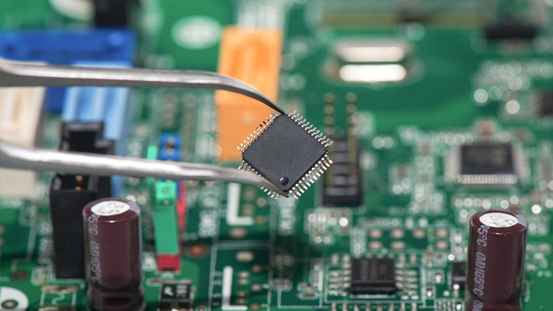
Rigid PCB assembly
Posted:09:52 AM January 13, 2020
writer: NextPCB
PCB assembly, also known as PCBA, is a process of mounting various electronic components to a PCB. The board is called a PCB before assembling the electronic components on it. After the electronic components have been welded together, the board is called a PCBA. There are several assembly ways for rigid PCB, through-hole technology(THT) and surface mounting technology(SMT) are the main methods of PCB assembly.

Although SMT is the mainstream technology of electronic assembly, THT still plays a vital role in the assembly process due to the large size of some components in PCBA processing. So, there are a certain number of THT components in the PCB. The assembly of both THT and SMT is called a hybrid assembly, and the assembly using all SMT is called full-surface mounting. The PCB assembly method and its process flow mainly depend on the type of assembly components and the equipment conditions of the assembly.
Rigid PCB assembly process steps
What we usually call PCB assembly generally refers to the rigid PCB assembly, and the main steps are listed as below:
Step 1: Solder paste stenciling
Solder paste needs to be added to the area that the components will sit in the final PCB before placing components. The solder paste usually appears gray and must be applied to the board in the correct position with the correct amount.
Step 2: Placing components
SMT places components on the board primarily with pick-and-place machines because of the high requirements for accuracy.
Step 3: Reflow soldering
In this step, the actual connection takes place. After the components are put, the board is placed on a reflow furnace conveyor. The solder applied during the soldering process melts during reflow. Then the PCB passes a series of cooler heaters to allow the molten solder to cool and solidify in a controlled manner, which will connect the component to the board permanently.
Step 4: Waving soldering
If there are through-hole components or PTH components, waving soldering is needed. In this step, the board is placed on a mechanical conveyor driven system and passes through different areas of the PCB through the melt welding wave, which helps connect the PCB pads/vias, electronic components lead, and solder. Then the electrical connection is formed.
Step 5: cleaning
It is important to clean the PCB after assembly, which helps to clean all flux residues with the deionized water. This step also can be done after the inspection process.
Step 6: Inspection and functional test
Usually, movement during the reflow process results in poor connection quality or total connection loss. Short circuits are also a common side effect of this kind of movement because misplaced components sometimes connect parts of the circuit that should not be connected. So, the final step is testing the functionality of the PCB to identify any potential problems and fix them as soon as possible. Manual checks, automatic optical inspection, and X-ray inspection are the conventional inspection methods to check for these errors and misalignments.
 PCB Assembly
 Layer Buildup
 Online Tools
 PCB Design-Aid & Layout
 Mechanics
 SMD-Stencils
 Quality
 Drills & Throughplating
 Factory & Certificate
 PCB Assembly Factory Show
Certificate

