Panel Requirement for Assembly
Posted:05:03 PM December 18, 2019
writer: NextPCB
As we all know, the size of the PCB panel is significant for the SMT assembly process. If the single board or panel is too small or too large, they cannot be brought to the rails on SMT lines. Most of the time, the panel size of PCB fabrication is different from PCB assembly size.
Benefits of PCB panel
When the size of the PCB is not suitable for fabrication, PCB manufacturers need to panel the PCB on a big board. What are the benefits of panel design?
Firstly, more odd PCB shapes have existed because we need to pack the electronics into less space. We should nest or flip the PCBs for this case when making panel design to reduce materials waste and increase board utilization.
Secondly, the SMT machine works very fast due to the high automation, and it can place several components in only one second. Usually, it takes less than 10 seconds to complete all the assembly work for a single mobile phone PCB. Therefore, increasing the number of components by panelized PCBs can increase the utilization rate of the assemble machine and improve the efficiency and yield of fabrication.
Finally, it can save a lot of time when picking and placing PCBs because multiple boards can be taken at the same time. The labor time of picking and putting PCBs during tests also can be saved if the subsequent board test can be connected.
Several ways of panel design
1. V-scoring/V-cut/V-groove
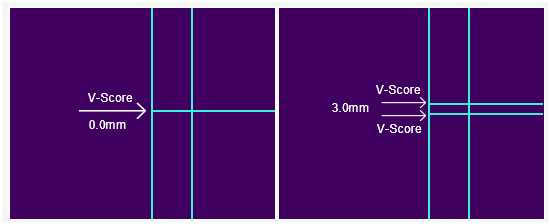
The space between each unit can be 0.0mm or 0.3mm for panel with V-scoring in the following picture.

Notes:
The machine will go through the whole board and no-stop when running the V-cut process, so straight edges can use V-cut techniques to minimize the amount of waste material, which is also easier to clean up.
2. Tab-route
The space between each board needs to be 1.6mm for panel with tab-route, and there are two types of tab-route as below:
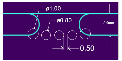
① Tab-route with breaking holes (stamp holes)
The space between each breaking hole should be bigger than 0.5mm, and the diameter of breaking holes also need to be bigger than 0.5mm. It is more suitable for about five or six breaking holes on each tab as the flowing picture.

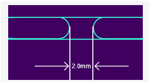
② Tab-route with the tab (no holes)
The space between each tab should be 2.0mm as the flowing picture.

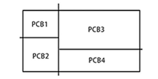
PCBA units with different sizes or shapes as the flowing picture cannot be paneled with V-cut. Tab-route is more suitable for this situation.

3. Combination of V-scoring/V-cut/V-groove and Tab-route
The space between each board should be 2.0mm when panel with both V-cut and tab-route. This combination way usually increases the production cost but reduces PCBA separating labor and lower the damage risk.
The minimum size of the PCB assembly panel in NextPCB is 50mm*50mm; the maximum size is 600mm*500mm. We can provide the panel design according to customers' requirements, or customers can offer panel design directly. Customers can choose the right selection when placing orders online. Leaving messages and send Emails for the panel design is also available.
 PCB Assembly
 Layer Buildup
 Online Tools
 PCB Design-Aid & Layout
 Mechanics
 SMD-Stencils
 Quality
 Drills & Throughplating
 Factory & Certificate
 PCB Assembly Factory Show
Certificate

