BGA (Ball Grid Array) is a type of semiconductor package. It features a grid of spherical pins on the bottom of the package, which are arranged in a lattice pattern, giving rise to the name BGA.
Many motherboard control chips utilize this packaging technology, which often involves the use of ceramic materials. Memory chips packaged using BGA technology can double or triple their capacity without increasing in size. Compared to TSOP packaging, BGA offers a smaller volume, superior heat dissipation, and enhanced electrical performance.
BGA Package Pad and Trace Design:
- Trace Routing Between BGA Pads: For BGA pad spacing of less than 10 mils, routing between them is not feasible due to trace width and spacing manufacturer limitations. To route traces, BGA pads should be sized accordingly to ensure adequate spacing between pads and prevent pads from being cut into irregular shapes, which could affect solder joint quality.
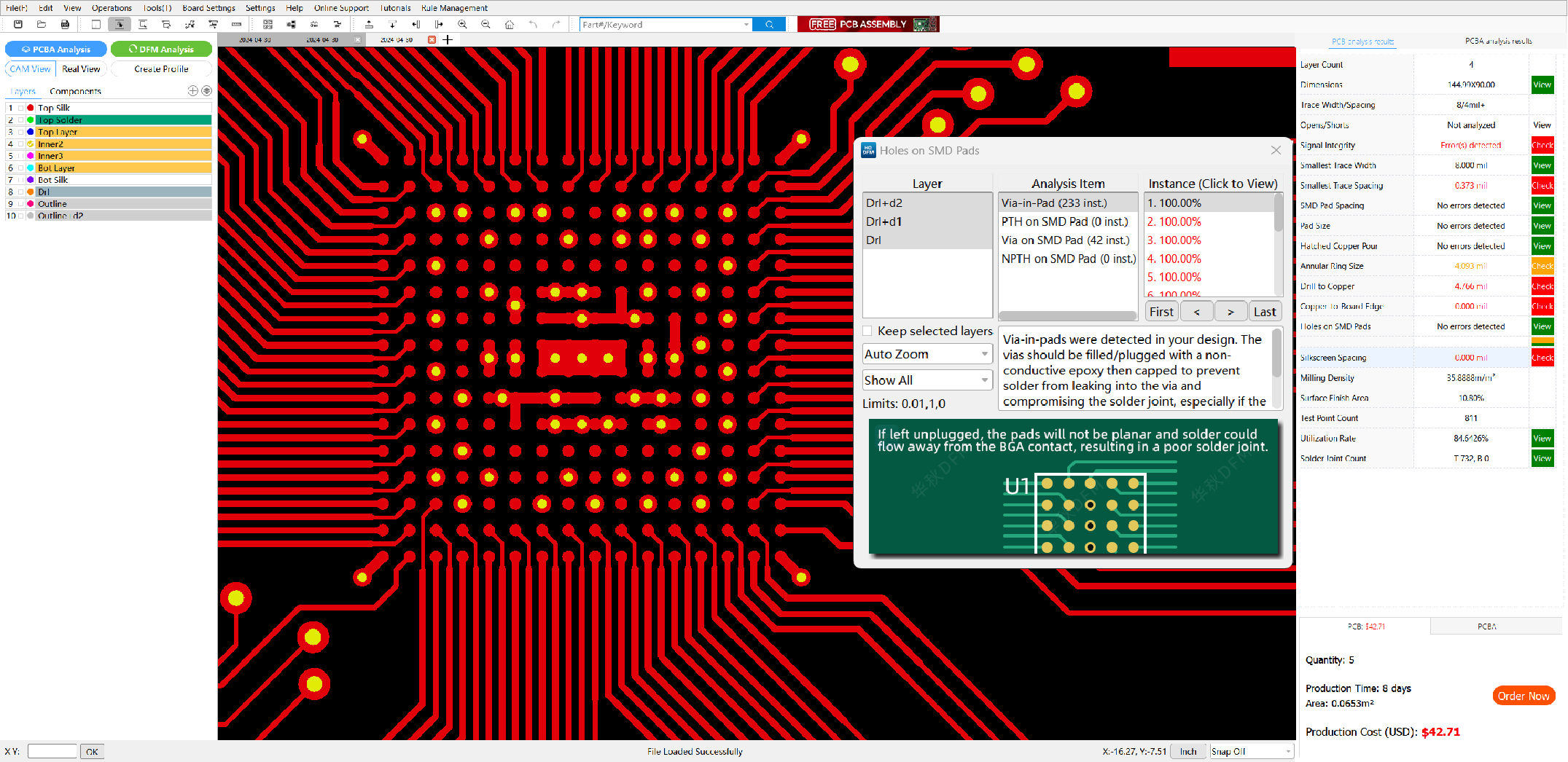
- Via-in-Pad via filling and capping: When pad spacing is tight and routing between pads is not possible, vias can be placed directly on BGA pads, allowing for signal transfer to inner or bottom layers. However, these vias must be filled with resin and capped. If not, solder joint defects are almost certain to occur due to the non-planar surface and solder leakage into the vias.
- Tenting of Regular BGA Vias: Vias between BGA pads typically require adequate covering. Considering cost and production complexity, solder mask tenting is usually sufficient for low demand applications and prototypes. Solder mask plugging can offer better protection against foreign material entering the barrel and improves via lifespan. Additionally, during reflow soldering, tented and plugged vias prevent solder from causing shorts on either side of the board.
- Via-In-Pad and HDI Design: For fine-pitch BGA chips where traces cannot be routed between pads, it is advisable to utilize a HDI (high-density-interconnect) design with blind and buried vias. For example, mobile phone boards typically have small BGA chips that do not allow for routing between pads. An HDI design with blind and buried vias can be used to make maximum use of the available space in all layers.
BGA Soldering Process Quality:
- Solder Paste Printing: The purpose of solder paste printing is to evenly apply the right amount of solder paste to the PCB pads to ensure good electrical connection and sufficient mechanical strength during reflow soldering. Solder paste is applied through the corresponding openings in a stainless steel stencil onto the PCB pads using a squeegee.
- Component Placement: Placement involves using a pick-and-place machine to accurately place components onto the PCB where solder paste or adhesive has been applied. High-speed placement machines are suitable for mounting small, high-volume components like capacitors and resistors, as well as some IC components. Universal placement machines are used for components requiring high precision or diverse shapes, such as QFP, BGA, SOT, SOP, and PLCC.
- Reflow Soldering: Reflow soldering melts the solder paste on the circuit board pads, which will mechanically and electrically connect the surface-mounted device terminals to the PCB to form an electrical circuit. Proper temperature curve settings are crucial for ensuring the quality of reflow soldering. Inappropriate settings can lead to incomplete soldering, cold joints, component warping, and excessive solder balls, impacting product quality.
- X-Ray Inspection: X-Ray inspection can detect nearly all process defects. By comparing the shape of solder joints against standard shapes stored in a computer, the quality of the solder joints can be assessed. This method is indispensable for inspecting solder joints on BGA and DCA components. It does not require test molds, although it is currently quite expensive.
Reasons for Poor BGA Soldering:
- Opened BGA Via-in-pad: Open vias on BGA pads that are not filled and capped can result in the loss of both the BGA solder ball and solder paste during the soldering process. The molten solder can leak through the barrel of the via, leaving insufficient solder to form a good solder joint.
- Inconsistent Pad Sizes: Variability in BGA pad size can affect the quality of solder joints. The width of the trace leading from the BGA pad should not exceed 50% of the pad diameter, and the trace width for power pads should be no less than 0.1mm. To prevent pad deformation and pads of varying sizes, solder mask expansion should not exceed 0.05mm.
HQDFM Solutions for Improving BGA Chip Solder Quality
- Via-In-Pad Design: HQDFM performs a one-click analysis of Gerber and OBD++ files and can detect the presence of vias-in-pads. HQDFM reminds designers that via-in-pads should be filled and plated to prevent solder defects and that this increases production costs significantly. If these can be moved away from the pad and converted to regular vias, this will remove the need for via filling and capping.
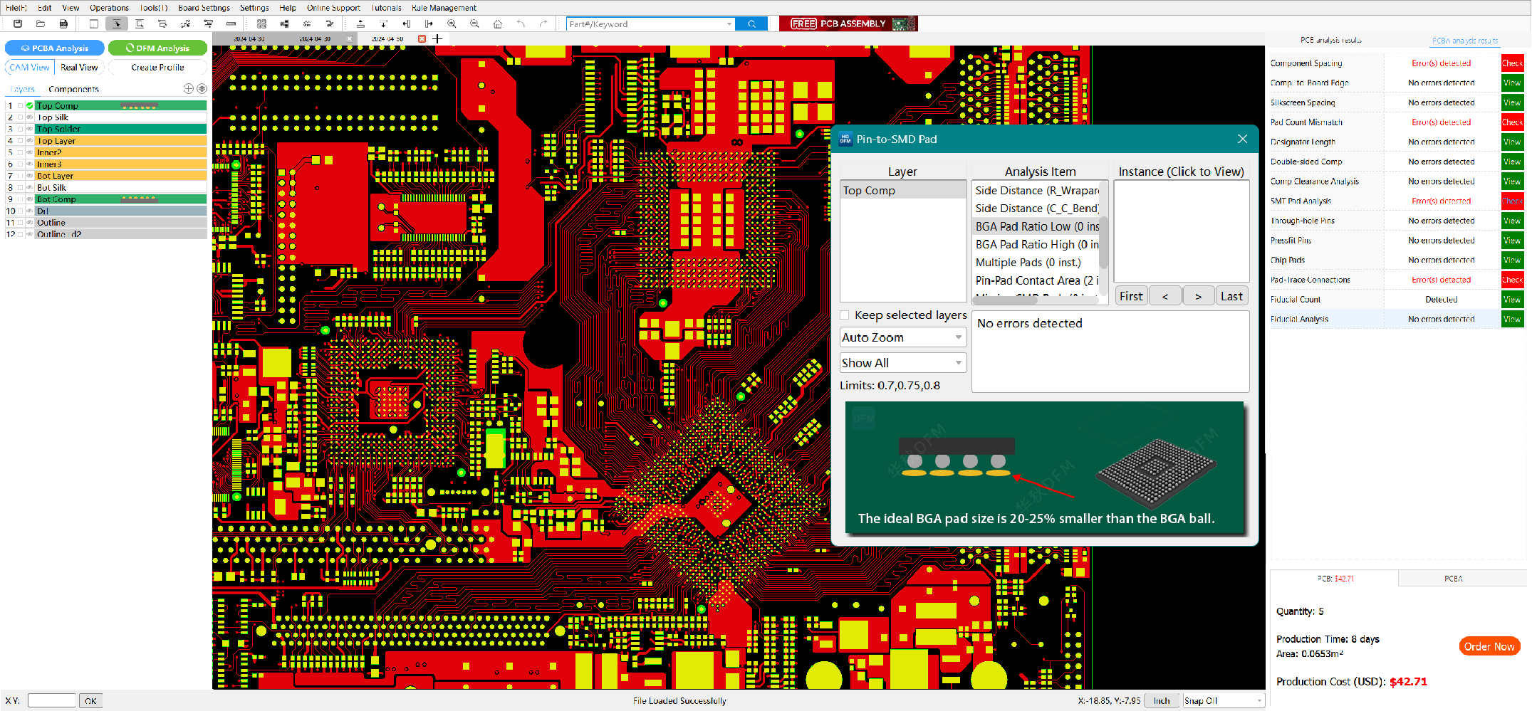
- Pad-to-Pin Size Ratio: HQDFM can compare the solder pad size to the size of the BGA ball. A pad diameter less than 20% smaller than the BGA pin size could lead to insufficient space for routing, while more than 25% might result in poor solder joints. In such cases, design engineers need to adjust the ratio of pad diameter to BGA pin diameter.
HQDFM offers solutions to improve the solderability of BGA chips by helping users review the BGA design before production, thus preventing solderability issues during assembly. It also provides indications of the effect on yield due to BGA pad design choices.
HQDFM Online Gerber Viewer


