
Support Team
Feedback:
support@nextpcb.comProduct developers are well aware of the challenges involved in producing a product fit for the market. Even the most experienced designers have to go through numerous prototype iterations before coming to a mass-production version.
The Design for X, or Design for Excellence methodology divides the various aspects of product design into distinct disciplines, from Design for sustainability, Design for cost, Design for testing, Design for Manufacture and Assembly and others. It advocates a systemic checklist approach to product design, as opposed to the traditional linear approach which is susceptible to costly, hidden errors and lengthy development cycles.
DFX is based on the concept that the earlier problems are found during development, the easier they are to fix. Thus, DFX can help reduce the number of product iterations required until the desired product is achieved.
As manufacturing and assembly experts, it is our obligation to help our clients achieve perfection first-time round. This is why we actively perform Design for Manufacture and Design for Assembly for our clients and promote DFM and DFA methodologies in the form of self-service tools. The benefits are mutual, as fewer errors in the design reduce complications and delays on the factory floor, and clients receive their products with minimal disruption and errors.
HQ NextPCB’s PCB production facilities have always been coupled with a mandatory engineer Design for Manufacture file review, and NextPCB pride themselves in providing some of the most comprehensive and consistent DFM review services in the industry. This year, NextPCB introduced the Design for Assembly engineer review service, free with the turnkey PCB Assembly service for the same purpose.
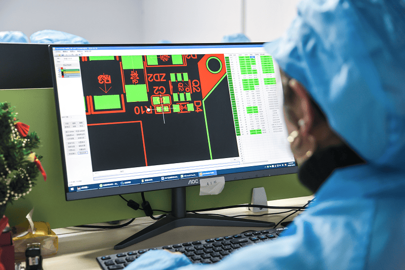
Design for manufacture for PCBs ensures that the production data is sufficient to produce the circuit boards and that the specification is within the manufacturer’s capabilities, at the same time, NextPCB engineers also report other anomalies that may be design mistakes, such as shorts, missing drill holes and pads, etc.
For Design for Assembly, engineers look at the assembly documentation, including the Bill of Materials, pick and place data and other supporting documents to verify they understand the assembly requirements and that the design data is consistent. At the same time, they confirm each and every footprint in the design with the help of internally developed software and make a note of details technicians later in the production phase must be aware of, such as special assembly requirements and panelization requirements.
With special training and tools, DFA engineers can help clients reveal mistakes in the design that may prove very costly in both terms of time and money. To give you a better idea, here are some real examples of some DFA problems and the impact they were not identified.
Problem Type: Footprint mismatch
Problem description
The client's design has the land pattern for a 0806 chip resistor, but the BOM file requests a chip size of 0402
DFA Solution
1. Change the footprint
2. Substitute the part in the BOM file for a 0805-sized part
Solution if found at the assembly stage
1. Find and purchase a 0805-sized version of the part.
2. If no suitable replacement can be found, the PCB boards have to be modified and reproduced.
3. Force solder the part
Complications
1. Cost of purchasing replacement parts. If the part requires importing, this may take weeks to arrive, causing significant delays to the project.
2. Cost of re-producing PCB boards. If other parts on the boards have already been soldered and cannot be salvaged, the parts will have to be scrapped and purchased again, essentially starting the entire PCBA process from scratch.
3. Force soldering may not be possible if the difference in size is too great. If possible, force soldering could cause the defect rate to increase and affect the reliability and lifetime.
Comments
For resistors and capacitors, substitutes are more readily available, however, for parts like chips, the chances of finding a swap-in replacement are much lower.
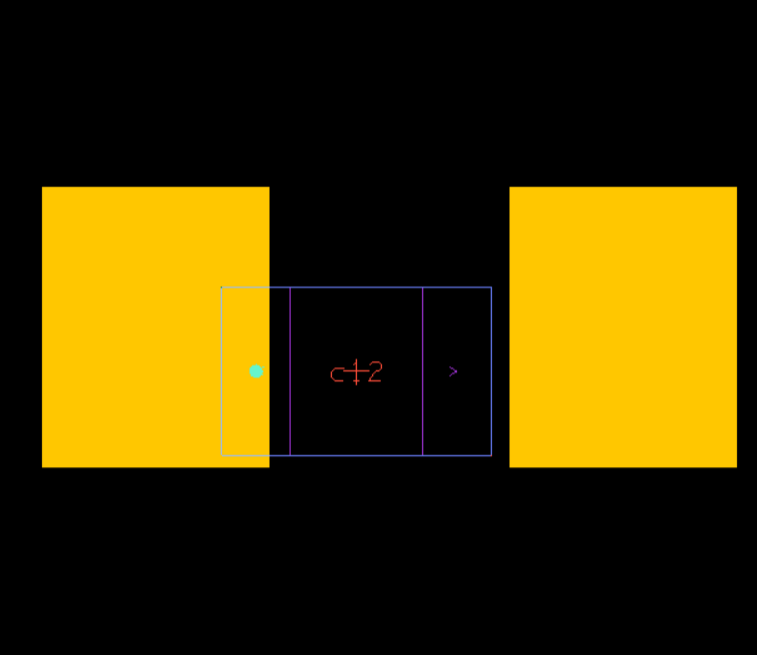
Problem Type: Footprint mismatch
Problem description
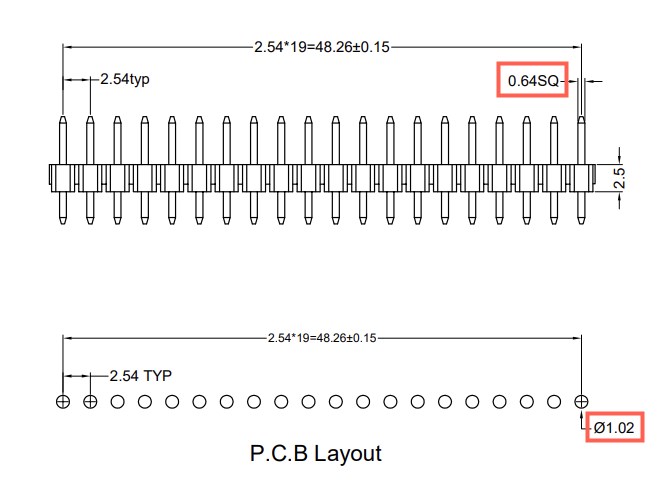
Client's design requires headers with square-shaped leads of width 0.65mm. Seeing the value of 0.65mm in the datasheet, the client adds holes with a finished diameter of 0.75mm, forgetting that the diagonal length is actually √(0.64² x 0.64²) = 0.905mm. As a result, the headers cannot be inserted.
DFA Solution
1. Change the footprint
2. Substitute the part in the BOM file for a header with slimmer leads
Solution if found at the assembly stage
1. Best case: Find and purchase a header with slimmer leads.
2. Worst case: If no suitable replacement can be found, the PCB boards have to be modified and reproduced.
3. Force solder the part
Complications
1. Cost of purchasing replacement parts. If the part requires importing, this may take weeks to arrive, causing significant delays to the project.
2. Cost of re-producing PCB boards. If other parts on the boards have already been soldered and cannot be salvaged, the parts will have to be scrapped and purchased again, essentially starting from scratch.
3. Force soldering may not be possible in all cases and will depend on the manufacturing tolerances. Force soldering could damage the wall of the plated hole or the component, causing the defect rate to increase and affect the relibility and lifetime. Additional processing fees may be significant for large volumes.
Comments
Many headers come with standardized lead widths, so the chances of finding an exact replacement are very slim.
In the standard soldering process, through-hole parts are soldered after surface mount parts have been reflowed. So if the through-hole parts have not been verified beforehand, starting from scratch is a very real possibility.
Problem Type: Footprint mismatch
Problem description
Due to errors in Gerber file generation or footprint conversion, the milling slots for a micro USB port have not been exported in the Gerber files, and the part cannot be inserted.
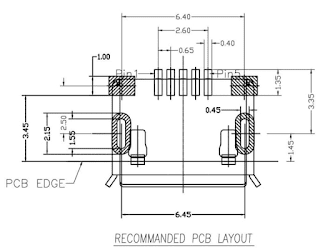
The footprint has drill holes instead of milling slots
DFA Solution
Investigate the issue and re-export the Gerber files with the milling slots
Solution if found at the assembly stage
1. Re-produce the PCB boards
2. Force solder the part e.g. cut off the tabs on the USB port
Complications
1. Cost of re-producing PCB boards. If other parts on the boards have already been soldered and cannot be salvaged, the parts will have to be scrapped and purchased again, essentially starting from scratch.
2. Cutting off the tabs weakens the strength of the mechanical connection to the board which may cause the port to come loose with repeated use. Also, for large quantities, cutting the tabs may incur significant handling fees and extend the deadline.
Comments
Almost all micro USB ports have wide tabs that require slots so finding a substitute with no tabs or round tabs is near impossible.
Due to a lack of support for slots in some popular PCB design software and poor footprint imports, this problem is much more common than you might think.
These are just some of the issues DFA review can reveal. To really appreciate how DFA review can save you time and money, you have to just try it for yourself. Now, HQ NextPCB offers DFM review as part of their turnkey PCB assembly service as standard, and with the free assembly service for 5 pieces and fast quotation platform, trying NextPCB PCBA is easier than ever. Visit HQ NextPCB to learn more.
HQ NextPCB PCB Assembly Services
Still, need help? Contact Us: support@nextpcb.com
Need a PCB or PCBA quote? Quote now
|
Dimensions: (mm) |
|
|
Quantity: (pcs) |
|
|
Layers: |
Thickness: |
|
|
|


