Support Team
Feedback:
support@nextpcb.comIntroduction
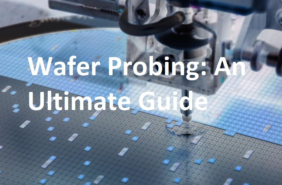
Dies were made in different packages, and these dies were passed through the wafer probing test. The main purpose of this test is to find an inefficient wafer, that offers the best result, which can affect the production of wafers, quality control, and manufacturing process control. For this test, the instruments used are known as wafer probers. Wafer probing machines are automated testing instruments used in the semiconductor manufacturing process for electrical tests of integrated circuits of different wafer dies. Two probes are used to measure different electrical features of the transistor, connection, and other components during their movement from one IC to another.
This test is done in the integrated manufacturing process on each silicon die and wafer. If this is not performed, defective dies can affect the whole assembly process and result in a high-cost manufacturing process.
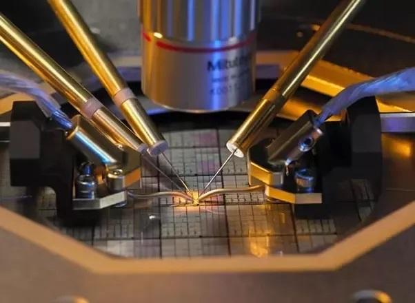
Wafer probing is a method for developing and producing semiconductors that test each wafer electrically. For this test, an automated probing system was used. This machine holds the wafer on a stable mount and uses tin pins, which are used for accurate point pins. These probe pads, also known as contact or connection pads, connect wafers through the use of accurate point pins.
The probe system is normally attached to a piece of automated test equipment that handles the needed electrical tests on every die. The test instructions connected to pins offer each through voltage, testing the accurate function of every chip at the same instant. Probing is performed to make sure that the wafer is not defective in low-electric products, and that the wafer is made in different units, saving on testing and assembly costs.
Wafer probing is very important for microelectronics and semiconductor production. To find the features of prototype ICs, manual wafer probing is used, which finds different defects. With that, it provides highly accurate calculation and evaluation of TEG for ICs made of transistors, connectors, etc. For assessing wafers at low and high temperatures, the wafer probe comes with temperature control features. Automatic wafer probing is needed for semiconductor large manufacturing testing to ensure accurate placement and high-speed controls in the TEG testing process. During an inspection of wafer ICs for errors, the probe performs removal or continues the assessment.
It is a map that is used for revealing die passes and no passing with the use of bins. The bin will be defined as good or bad dies. The wafermap will move electronically for the assembly house that just picks passing dies by choosing the bin number that has good dies. In older days, good dies were mentioned with ink dots, but this process is not now common. The use of ink dots helps with visual inspection since the operator cannot select the die based on the ink dot. While only dies that pass all test patterns used When a component's defects don't materially affect the device where it will be installed, it may be included even if it didn't pass every test pattern.
This process involved the wafer probing system application for electrical testing of wafers on each chip. The wafer probe loads and correctly positions the wafer wafer chuck, which is a round-shaped plate. The wafer is moved into electrical contact using small needles known as probe cards. The devices now get test signals transmitted from instruments and sent back. In simple words, test signals from measuring devices are sent to single devices on the wafer with the use of connected probe needles or probe cards, and signals are then again sent to devices.
Instruments for the wafer probing process are explained here.
For test preparation, automated test equipment is arranged with other components such as a probe card, load board, handler, DUT board, wafer probe station, and other instruments.
In this step, design features, and test details are given in the datasheet for the creation of the test plan and the making of test processes. The probe structure should be made correctly, and high-power features should be configured according to need.
The wafer probe aligns the bonding pad of the wafer through the needle in the probe card. It comes with a wafer holder holding the wafer and a photoelectric detector for the detection surface of the wafer to get details of the proper alignment required to configure the bonding pad with a probe pin in horizontal and vertical alignment.
The different types of wafer probing systems used are explained here.
DC probing is an important feature of wafer testing that evaluates the direct current features of ICs. In this process, certain features like current, resistance, and voltage are measured to ensure the accurate working of the semiconductor device. DC probing is an instrument for identifying any changes in required electric features to help find and solve errors at the start of the manufacturing process.
The full form of RF is radio frequency probing, which is a certain type of wafer testing that is configured for the assessment of the high-frequency operation of ICs. This problem is important for wireless communication devices. RF probing helps to find the signal quality and frequency repose for the good function of devices operating in radio frequency ranges. By putting semiconductor devices into RF probing, engineers can make sure that these components are according to the needs of projects like radar systems, wireless communication, and different high-frequency methods.
It is an important factor in wafer testing that checks specific features of integrated circuits. This process involves transistor feature analysis, resistance, capacitance, and other electrical features. This probing helps to get complete details of the nuanced operation of semiconductor devices to make sure that these components fulfill the accurate features in the designing process. Through analyzing the features, any changes from the required values can be found at the starting phases of the production process, which helps to solve them at the start and make changes if needed.
Wafer-level reliability testing methods are used to offer high-speed process control data for processes that can cause premature IC damage and affect the operation of the device. This test is used to measure changes in materials used to make devices and streamline new integrated circuit designs and process identification by detecting the reliability of the process. Through functioning the device at its best, this test helps the device's operating life for a known damage process. These tests are performed on the built-in structure of the wafer to get data and make sure they can be performed at the start of the manufacturing process.
This testing process is important for ensuring the function, quality, and reliability of ICs. It involved different phases to find errors, operation evaluation, and checking that devices were according to the required standards. Here are some semiconductor testing processes explained.
This process involves the testing of single dies on a semiconductor wafer.
When wafer probing is performed, dies are assembled and packaged in semiconductor devices.
This is done to evaluate the function and reliability of completely packed devices. The testing performed is mentioned here.
This is done to evaluate temperature and electrical stress to find faults at an early stage.
It is used to determine the long-term operation of the device under different conditions.
It is used to sort devices based on quality.
It is used for test result analysis and making detailed reports.
The basic use of wafer probing is in semiconductor device testing. Since it is the main step, each die goes through certain tests to verify function and operation. Semiconductor device testing makes sure that only high-quality components move to the next steps of manufacturing. By finding the faults at the start of production, we can increase production rates and provide reliable devices to customers.
Wafer probing is an important part of the analysis of semiconductors in manufacturing. With detailed testing, this process helps to find the main causes of errors in semiconductor devices. The detailed results of the failure analysis help to increase the production process, avoiding the same error in the future and making sure the manufacturing of high-quality and error-free components
This method is like failure analysis. The main objective is to check that either chip design was made correctly, as there can be errors in the manufacturing process that can cause defects. Due to these causes, the chips are screened through wafer probing, where the IC is fired up with probe cards, and micro-probing is done through different single probes at the same time. It is done at the wafer level, while other verification methods like burn-in tests, characterization, structural tests, and functional tests are performed at different points of manufacturing.
|
|
|
|
|
|
|
|
|
|
|
|
|
|
|
|
|
|
|
|
|
|
|
|
|
|
|
|
In the process of semiconductor manufacturing, wafer probing is the cornerstone to ensuring the functionality and quality of ICs. Through systematically testing single dies on wafers, engineers can find and solve the different errors in manufacturing. It not only increases the production rate but also helps to provide high-operation devices that fulfill the need for the latest technologies. As technology continues to advance, wafer probing is also important for the semiconductor industry.
- IPC-J-STD-001: The Standard for Soldering Assemblies
- IPC-A-600: The Standard for Printed Circuit Board Inspection
- Free PCB Assembly Offer is Now Live: Experience Reliable PCB Assembly from HQ NextPCB
- HQ NextPCB Introduces New PCB Gerber Viewer: HQDFM Online Lite Edition
Still, need help? Contact Us: support@nextpcb.com
Need a PCB or PCBA quote? Quote now
|
Dimensions: (mm) |
|
|
Quantity: (pcs) |
|
|
Layers: |
Thickness: |
|
|
|