Support Team
Feedback:
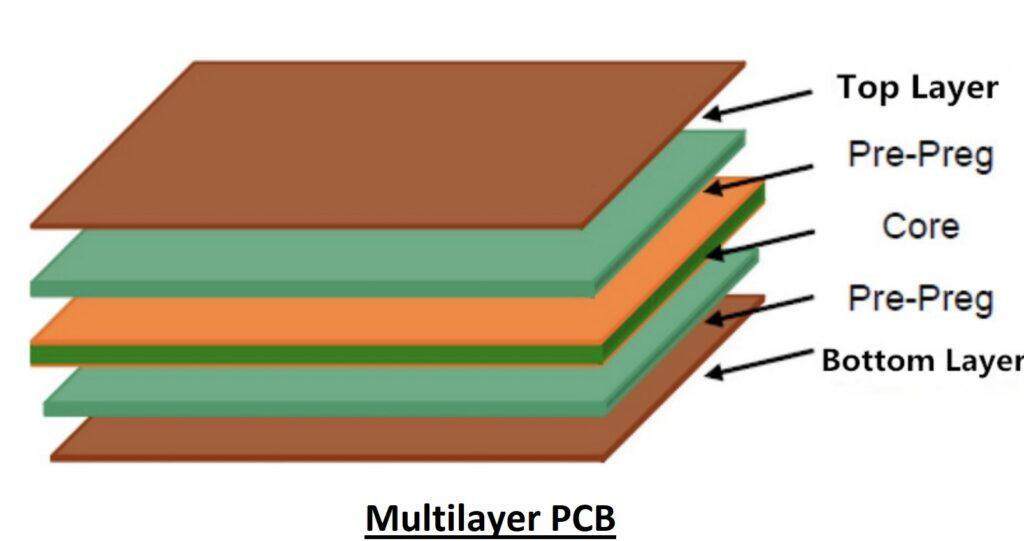
support@nextpcb.comMultilayer boards are now the main component of electronics since their features are high density, good signal quality, and effective heat management. Currently, electronic devices are creating some complicated circuits, so multilayer board design is the main factor in ensuring their operation and reliability. Multilayer boards come with more than two copper layers. It comes with at least three conductive layers of any conductive material, mostly copper. All layers are connected with copper-plated holes, PCB vias, and laser micro vias.
Multilayer boards are configured with copper foil, prepreg or adhesive, and core materials. All these materials are under pressure to remove the air, and heat is applied to cure the adhesive that firmly connects the PCB layers. Here we'll cover the details of the multilayer PCB design and factors that are important for design. So let's get started.
The different steps involved in the manufacturing of multilayer boards are explained here.
Here are some points explained that consider making the board layer stack up.
Performance
The circuit function speed and operation condition of the board can be different depending on the materials that the board will use for board creation. Some of the latest materials, such as FR4, can be best suited to project needs, but these materials can also affect different parameters, like impedance measurement. So the best PCB manufacturer will be beneficial for you.
Cost:
The materials of multilayer board with layer court and arrangement will affect the cost of board creation. For the cost estimation, you must discuss it with your PCB manufacturer.
Density:
The routing density of the board is also the main factor in defining the board layer stack-up. It will be annoying for you if you have to add board layers again when you are already working on the board layout. You not only have to rearrange CAD data, but you also have to make many changes in layout. If there are many layers, there will be a high cost.
Circuit:
There is a need to understand the circuit to make an optimized layer design. Such sensitive signals need a stripline layer design for accurate operation, which will add extra ground planes. There must be a separation between analog and digital circuits with their ground planes, and power sources on board must also be separate. All these features will affect the layer arrangement, and it must be planned before starting the layout.
Signal Integrity
Sina integrity is the quality of the signal sent through traces on board. Different parameters, like impedance control, transmission line effects, and EMC parameters, affect signal integrity. So we must consider the route of a high-speed signal to avoid reflections and reduce noise to ensure accurate signal transmission.
Power Integrity
It is the main factor in the stable and accurate working of electronic circuits. Designing an accurate power distribution network, connecting the decoupling capacitor accurately, and optimizing the power plane design are the main factors in multilayer board design to reduce voltage loss and round bounce to solve power-related issues.
Thermal Considerations
The dissipation of heat is important for the reliability of electronic circuits. It is best to accurately connect components, accurately make thermal vias, and use copper pours effectively to regulate and avoid overheating, especially in applications where high power and temperature are involved.
Layout Considerations
Effective operation of a multilayer board is based on accurate component configuration. It is best to consider facts like routing methods and accurate component positions and follow the clearance and spacing instructions to ensure good signal transmission, less noise interference, and simple assembly and testing methods.
Design for Manufacturability (DFM)
Make sure the multilayer board is made according to manufacturability to avoid high-cost rework and delays in the production process. Panelizaion solder mask application and copper balance are the main DMF factors that must be accurately performed. An accurate penalization process, proper solder mask design, and balanced copper distribution are important features of well-optimized manufacturing and assembly that minimize the different faults and ensure smooth manufacturing flow without any high-cost damage.
The accurate multilayer board design comes with accurate component connection and routing, accurate documentation in manufacturing drawings and output files by following the DFm rules, and the use of the latest design software for analysis. The support of expert manufacturers and continuous refinement of the design process help to ensure accurate manufacturing of quality multilayer boards.
The detailed approach makes sure that the design fulfills functional and manufacturing needs, resulting in a reliable and manufacturable multilayer PCB. The interval discussion with the manufacturer is important to explain any certain needs or suggestions that are needed for the process and have required board
What is the importance of component placement in PCB layout design?
The placement of components is the main factor in making a reliable and well-operating board. The accurate placement of components also helps with effective routing traces, making a board of optimized size, and it also helps to manage EMI and thermal management.
What are the rules for multilayer PCB design?
The multilayer board must have at least three conductive layers made with conductive material. All layers are interconnected with copper-plated holes, like NC vias and micro vias.
How can simulation tools help in board layout design?
Simulation tools are best to get an idea of the operation of the circuit and find any faults existing on the board before manufacturing. These tools simulate the power distribution, thermal performance, and signal quality, which helps optimize the board design.
What materials are used in multilayer PCBs?
There are three basic raw materials used for manufacturing rigid multilayer boards: resin systems, reinforcement materials, and copper foil. The board is mostly made with the use of glass mechanical strength, and its main operation is to carry resin.
What are some challenges faced by designers in PCB layout design?
Some main challenges are heat management, EMI, component connection, DFm, design rule checking, different layer management, etc.
What is the role of CAD tools in PCB layout design?
It comes with some of the latest features of designing and board simulation, which help to accurately control the layout and component routing and traces. They also come with the latest simulation features that help check the board's operation in different conditions.
How do you identify a multi-layer PCB?
Multilayer board comes with more insulation layers sandwiched between copper layers. Count the insulation layers that help to find the number of layers of the board.
- The better the layer stack design, the higher level the PCB design
- Introduction to a KiCad demo project
- Free Worldwide Shipping on Over 600,000 Electronics Components with HQ Online
- Free PCB Assembly Offer is Now Live: Experience Reliable PCB Assembly from HQ NextPCB
- HQ NextPCB Introduces New PCB Gerber Viewer: HQDFM Online Lite Edition
Still, need help? Contact Us: support@nextpcb.com
Need a PCB or PCBA quote? Quote now
|
Dimensions: (mm) |
|
|
Quantity: (pcs) |
|
|
Layers: |
Thickness: |
|
|
|